
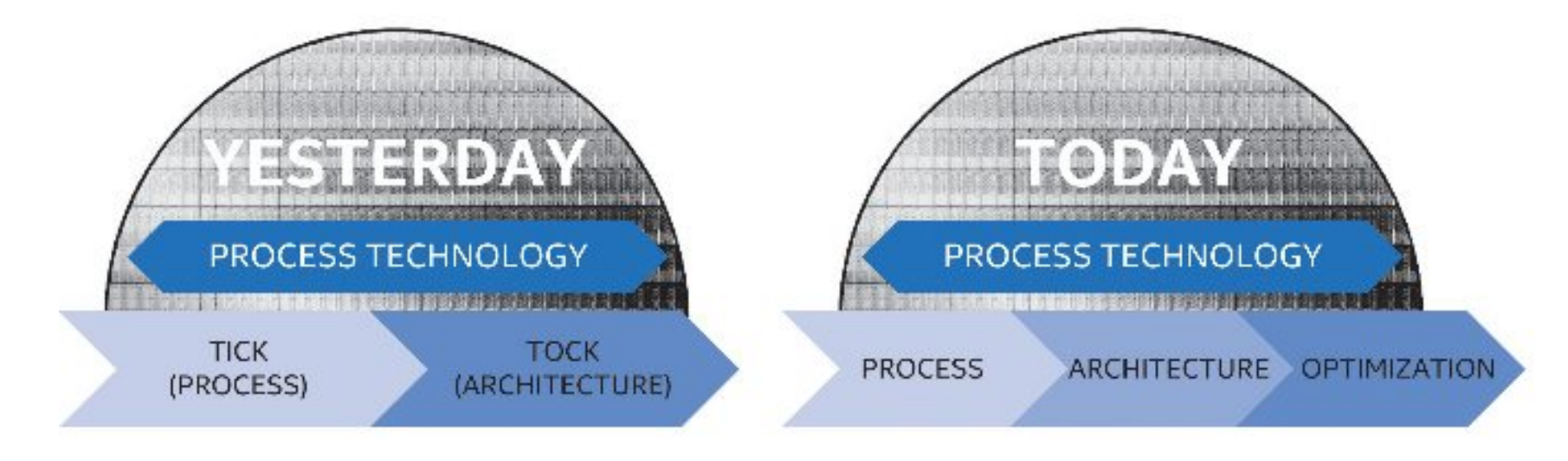
When Intel first announced the shift from the dual-stage ‘Tick-Tock’ methodology that had driven their core CPU design teams for over a decade into the three-way ‘Process, Architecture, Optimization’ paradigm, there were questions as to how much of the final stage, the Optimization, would actually change the way CPUs were presented or offer upgrades in performance. At the time, ‘Kaby Lake’ as the name for Intel’s third crack at their 14nm process was well known, but users wondered if it was just another Devil’s Canyon (better overclocking) or a full on CPU launch. Well the answer is the latter, and the launch is staggered between today and January. Roll on Kaby Lake. Is that Kah-bee Lake, or Kay-bee Lake?
Tick-Tock to Process-Architecture-Optimization (PAO)
Intel’s two year processor cadence of Tick-Tock allowed the company to alternate reducing the lithography node (a tick) with an upgraded microarchitecture (a tock) with modest gains of performance. Each stage of the Tick-Tock would take 12-15 months, with new lithography nodes taking longer and longer to reach maturity. Eventually it has gotten to a point where 14nm took too long to become pervasive in Intel’s product stack. For a manufacturing company and a CPU company, slowly rolling out Broadwell notebook and low power parts and then gutting the mid-range desktop was the result of the troubles of bringing 14nm to the prime time. Now in 2016 we have the launch of full-sized Broadwell-EP server parts running up to 22 cores in a 145W envelope, but the low power parts are a couple of microarchitectures ahead. We have this strange situation of a stretched landscape, partially driven by markets but also for manufacturing.
The move from Intel’s 14nm process to 10nm is a long, slow burn, taking much longer to develop than any process previous. We first saw 14nm in Broadwell mobile CPUs in Q3 of 2014, almost two years ago, and 10nm still isn’t on any public roadmap for early 2017. With the tick-tock strategy, and the launch of Skylake in mid-2015, this would leave Intel without a new CPU launch for almost two years, which is unheard of from Intel. Also, Intel’s partners rely on product cycles to announce and launch new products to generate revenue. To fill the gap, plus with a few other techniques, Intel moved to Process-Architecture-Optimization, or PAO for short.
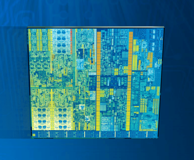
This means three bites of the cherry for 14nm before we see 10nm in prime time. First it was Broadwell, then Skylake, and today Intel is announcing Kaby Lake. As part of the release, Intel has mentioned that a number of key benefits for Kaby Lake will be based on an optimized 14nm process, called 14PLUS (or 14nm+, 14FF+). This process as a quick summary has a higher fin height and larger pitch, essentially giving a less-dense set of transistors that have more room to breathe. Normally a larger pitch means more voltage required, but this is offset by the fin height and Intel says is good for another few hundred MHz for performance. The less-dense design, in theory, may also help in overclocking, however we will have to wait until January to see those results.
Today’s Announcement
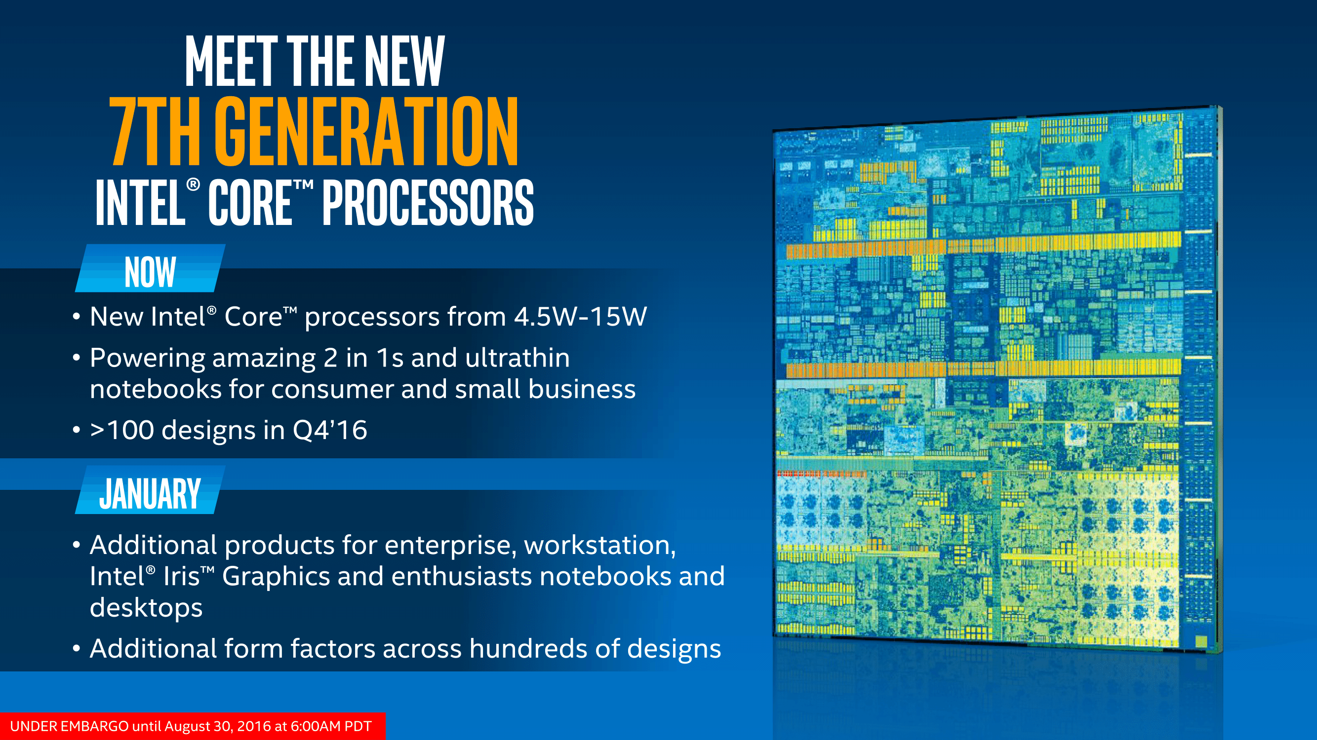
The reveal today covers several aspects of Kaby Lake. First is the actual SKUs that will be launched, which consist of three Kaby Lake-Y parts around 4.5W aimed at high-end tablets and 2-in-1 devices and three Kaby Lake-U parts at 15W for notebooks. Both sets of KBL-Y and KBL-U CPUs will feature in mini-PCs as well, so we expect to see the usual array of Zotac and ECS announcements in due course. We have details on all six CPUs to give you, including the new Core M branding regime for the 4.5W family of parts.
The pre-briefings we have had go into some detail regarding changes in the processor, particularly regarding the new enhanced media blocks inside the GPU to support new encode/decode features. The graphics power, in terms of EUs or the microarchitecture, hasn’t changed but the fixed function hardware has some nice upgrades for an updated version of Gen 9 graphics aimed at the upcoming era of 4K support. Ganesh has gone into detail for us over what that means, especially where power and battery life is concerned for anyone creating/consuming 4K content.
Kaby Lake also has an updated Speed Shift package, to accelerate the work already done with Skylake in boosting the performance of the CPU quicker to save power. Intel call it a refinement in the mechanism of handing frequency control back from the OS to the CPU, however ‘Speed Shift v2’ is an adequate moniker to show the upgraded difference.
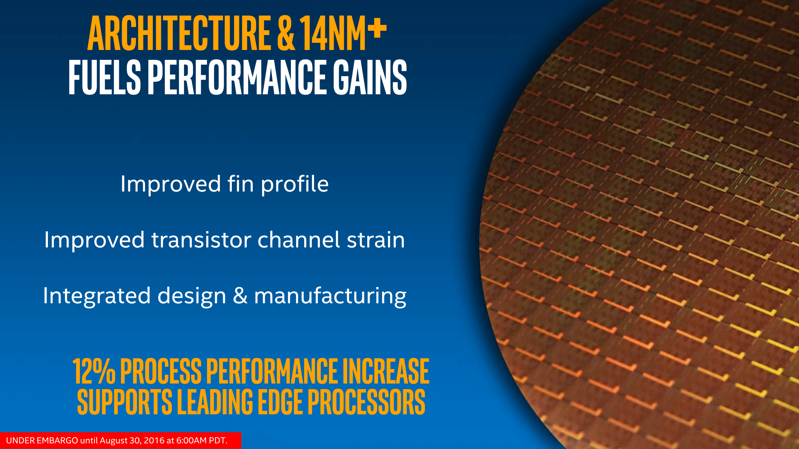
Intel hasn’t gone into much detail regarding the new 14nm+ process itself in terms of specifics, but has listed a number of performance gains that come out of the new CPU. The fundamental microarchitecture between Skylake and the new Kaby Lake parts is practically unchanged (DMI 3.0 now allows PCIe 3.0 x4 NVMe drives from the integrated PCH), but the updated fin profile and reduced ‘strain’ by the larger fin pitch is being quoted as giving a 12% performance increase due to process alone, typically through additional frequency for the same power. The main benefits to KBL will be in that frequency due to the 14nm+ process as well as the new media capabilities.
As always, Intel consistently emphasizes the difference between a new notebook/2-in-1 based on a 15W Kaby Lake processor compared to a 5-year old device, such one based on a mobile Sandy Bridge ULV part. Intel continually sees its market revolving around new experiences created by new form factors, and to generate revenue requires people to upgrade and decide how these new experiences can influence an upgrade. Intel expects to have over 100 Kaby Lake system designs in the consumer channel by Q4, including 120+ using Thunderbolt 3, 100+ using Windows Hello (either via a Real Sense camera or a fingerprint sensor), 50+ designs with 4K UHD as a primary feature and 25+ designs with contact enabled pens. Kaby Lake should be pin compatible with Skylake based designs, meaning that for a number of cases we will simply see a drop in, but others will have new design IDs on show.
One of the first things that users may notice about the new Kaby Lake processors is that the KBL-Y series is dropping both the m5 and my naming scheme from its segment. We will see m3 still, but this will now be paired with i5 and i7. Intel isn’t specifying that m5 or m7 have gone away entirely, but it doesn’t seem to be a part of the KBL-Y arrangement this time around.

There are a couple of reasons for this – the one Intel discussed with us is that it comes down to performance and OEM requests. An i5 in a 4.5W form factor (or as high as 7W in cTDP Up) performs essentially on par with the KBL-U i5 parts, and OEM customers requested that the naming scheme change to reflect that. The sense of parity and brand between the two, especially when customers look at a device for less than a couple of minutes and anything that they feel familiar with tends to be a bonus.
The other reason is perhaps that the Core M brand as a whole hasn’t taken off as Intel thought it would, or ‘m’ is associated with low power, low performance, or essentially ‘mobile’. So one could argue that renaming m5 to i5 is purely a mental adjustment tactic, however I’d hazard a guess and say that if they were called i5 and i7 to begin with, no-one would have batted an eye-lid at the difference. Interestingly enough, it is the i7 version of Kaby Lake-Y that has the highest single core turbo frequency mode out of all the processors being launched today, even the 15W parts. 3.6 GHz for a 4.5W TDP processor is nothing to be sniffed at, although it will depend on the device and OEM configuration that will determine just how long it stays at 3.6 GHz.
Finally, along with the change in how 4.5W parts are branded, Intel has also changed how this information is presented to consumers. The Intel case badge and similar marketing/identification material now includes the processor generation along with its designation. So instead of simply being a “Core i7” of unknown generation, Kaby Lake devices will be badged “Core i7, 7th Gen.” This should make it a bit clearer which devices are Kaby Lake versus Skylake, though it does raise the question over whether this will hurt Intel at all once Cannonlake (8th Gen) ships.

Skylake vs. Kaby Lake Branding
The Starting Lineup: 2+2
Like Broadwell in 2014, the 2016 launch of Kaby Lake is a bottom-up launch. This means that Intel is starting with the small die, low power Y & U series processors, and then will move further up the stack later on. So all 6 SKUs launching today – 3 at 4.5W and 3 at 15W – are based on the same 2+2 die. This means 2 CPU cores paired with a GT2 iGPU.

Intel has not disclosed the die size of their 2+2 Kaby Lake die at this time. This likely has something to do with the underlying 14nm+ process being used for Kaby Lake, which has left Intel a bit mum to start with (more on this later). At any rate, the Kaby Lake 2+2 die is not remarkably different in layout or design from Skylake. The big changes are under the hood: the 14nm process, and the GPU media processor improvements introduced with Kaby Lake.
The New Processors
Without further ado, here are the processors. First up, the KBL-Y 4.5W Parts, along with an m7 from Skylake for comparison:
| Intel 7th Gen (Kaby Lake) Y-Series Lineup | ||||
| i7-7Y75 | i5-7Y54 | m3-7Y30 | m7-6Y75 (Skylake) |
|
| Cores | 2 | 2 | 2 | 2 |
| Threads | 4 | 4 | 4 | 4 |
| Base CPU Freq. | 1.3 GHz | 1.2 GHz | 1.0 GHz | 1.2 GHz |
| Turbo CPU Freq. | 3.6 GHz | 3.2 GHz | 2.6 GHz | 3.1 GHz |
| Graphics | HD 615 (GT2) | HD 615 (GT2) | HD 615 (GT2) | HD 515 (GT2) |
| EUs | 24 | 24 | 24 | 24 |
| iGPU Freq. | ? | ? | ? | 1 GHz |
| TDP | 4.5W | 4.5W | 4.5W | 4.5W |
| DDR3L Freq. | 1600MHz | 1600MHz | 1600MHz | 1600MHz |
| LPDDR3 Freq. | 1866MHz | 1866MHz | 1866MHz | 1866MHz |
| Intel AMT & TSX-NI | Yes | Yes | No | Yes |
| Price | $ 393 | $ 281 | $ 281 | $ 393 |
Following on from the tradition with these low TDP parts, they all use a dual core, GT2 die with the low TDP numbers generated from the very low base frequency. Intel’s power management system allows for several states that dictate peak turbo frequency, frequency based on power draw, frequency based on skin temperature and thermal throttling. Most of the devices that use Y based processors are designed to offer a good turbo, either single core or dual core, until a certain SoC or skin temperature is reached. Kaby Lake carries on from Skylake in that Intel has increased the capability of the monitoring system to include more OEM-defined sensors and then use internal algorithms as appropriate. Kaby Lake also carries over gyro sensors that change that algorithm based on how the device is being held and what angle – a notebook on a table requires a different set of functions to determine frequency over time compared to a 2-in-1 being held horizontal or vertical, for example.

The Y series of CPUs will remain Intel’s attack on the high performance, low power market which takes advantage of a scalable microarchitecture but also the lithography advantage that Intel has over its competition. As a result, Kaby Lake-Y is similar to previous Y processors in that they will command a high premium. Even the base m3 processor runs a tray (1000 unit) listed price of $ 281, and 2-in-1s/notebooks with the similar Skylake parts over the past year have been running at the $ 600-$ 700 on the super low end. Mini-PCs have been lower, but still the premium over an Atom processor is palpable. It’s worth noting that the m3 variant does not support TSX-NI compared to the i5 and i7.

The i5-7Y54 mid-processor is actually listed as the same price as the m3, despite the increase in performance in the frequency and better instruction support. This is surprising, but hides any configurable TDP modes as Intel has chosen not to disclose these at this time. Chances are the i5 supports a high cTDP Up mode, but the m3 will support a low cTDP down mode.
The top end Core i7-7Y75 has the highest frequency of any Kaby Lake part in its turbo, at 3.6 GHz, and this is still super impressive for a 4.5W CPU. It all depends on implementation, and at $ 393 tray price, expect to pay a high premium for the privilege. The super-high-end 2-in-1 devices with Skylake, such as the Huawei Matebook paired with their top memory and storage configurations as well as keyboard, pen and extras, can cost in excess of $ 2000. This will undoubtedly continue for Kaby Lake this generation, with OEMs attempting to differentiate in style, design, and fight off the Apple factor. If Apple plans to update the new MacBook line this year, chances are that it will have the new Kaby Lake-Y as a direct slot in.
It’s worth noting that for all these Y parts, no exact figures for the graphics were provided. We suspect a direct parity with the previous generation for execution units given that we know it keeps Gen 9 and all three parts use the GT2 configuration (up to 24 EUs), however it will be interesting to see if the frequencies have increased due to the optimized 14nm+ process. There is also still no support for DDR4.
Next is the trio of Kaby Lake-U parts, with a nominal rated TDP of 15W.
| Intel 7th Gen (Kaby Lake) U-Series Lineup | ||||
| i7-7500U | i5-7200U | i3-7100U | i7-6500U (Skylake) |
|
| Cores | 2 | 2 | 2 | 2 |
| Threads | 4 | 4 | 4 | 4 |
| Base CPU Freq. | 2.7 GHz | 2.5 GHz | 2.4 GHz | 2.5 GHz |
| Turbo CPU Freq. | 3.5 GHz | 3.1 GHz | N/A | 3.1 GHz |
| Graphics | HD 620 (GT2) | HD 620 (GT2) | HD 620 (GT2) | HD 520 (GT2) |
| EUs | 24 | 24 | 24 | 24 |
| iGPU Freq. | ? | ? | ? | 1.05 GHz |
| TDP | 15W | 15W | 15W | 15W |
| DDR3L Freq. | 1600MHz | 1600MHz | 1600MHz | 1600MHz |
| LPDDR3 Freq. | 1866MHz | 1866MHz | 1866MHz | 1866MHz |
| DDR4 Freq. | 2133MHz | 2133MHz | 2133MHz | 2133MHz |
| Intel AMT & TSX-NI | Yes | Yes | No | Yes |
| Price | $ 393 | $ 281 | $ 281 | $ 393 |
On the face of it, the specifications of these three parts look similar to the Y series – dual core with hyperthreading, similar single core frequencies and similar pricing. What drives the TDP up is the base frequency, despite the use of Speed Shift technology (on Windows 10) to bring it down to more palatable levels when not in use. The point is that when the system is in use, it won’t drop below the base frequency, which is 2.4-2.7 GHz in this case, rather than 1.0-1.3 GHz for the Y series.
![]()
The Core i3, as with other i3 parts in generations gone by, has no Turbo Boost. This means that all cores and threads will run at a fixed frequency until idle or thermal throttling kicks in. The Core i5 and Core i7, while still dual core with hyperthreading, have Turbo Boost with an increase in both range and base frequency as we go up the chain.
Pricing for the 15W parts is identical to that of the 4.5W parts, with the justification still on the premium performance, but the thermal design means that ‘ultrabook’ style notebooks and NUC/BRIX like mini-PCs are more in line for these parts. Along with DDR3L/LPDDR3 support, we also get DDR4-2133 support with 1.2V modules – this will be an interesting point for users that end up gaming on these systems.

It’s worth noting that the Core i3-7100U also has a different implementation of the integrated chipset, or rather a cut down version (it’s still the same silicon underneath). The Core i3 loses RAID, a couple of USB 3.0 ports, PCIe 3.0 support (from the chipset, more on that later) and SATA ports.
This brings up a couple of things. First, I find it interesting that the m3 variant does not share this cut down feature set, meaning that the m3 products will still support RAID, PCIe 3.0 x4 storage and the like. Also, the fact that the Core i3-7100U and Core i5-7300U are the same price means that it is more of a platform play. With this cut down feature set, it requires a different platform design: an OEM cannot easily adjust the number of USB 3.0 ports on their motherboard and chassis just for one variant of a CPU, especially when the regular design supports both the Core i5-7300U and Core i7-7500U. As a result we might start to see fewer Core i3 variants on the market, except in devices where the limitations have little impact (ultrabooks).
OPI 2.0 to OPI 3.0
For anyone playing along at home, you may remember that during testing of a Skylake-Y NUC, we found that the PCIe 3.0 x4 slot for M.2 drives was actually limited to PCIe 2.0 x4, effectively reducing the peak bandwidth. At the time we probed Intel and our data sheets to find out that it was actually a limitation imposed by Intel on the CPU which wasn’t obvious from the original launch materials. The interconnect between the CPU cores/system agent and the integrated chipset, what we normally call DMI on a desktop platform but is called OPI on an SoC, was fixed at PCIe 2.0 speeds.
We asked about why this was the case, and we were told that the system actually can support PCIe 3.0 x4 speeds, and the system even tests this on startup, but for stability PCIe 2.0 is chosen. This made the marketing of the NUC a little confusing, especially as PCIe 3.0 x4 for storage was listed as a feature. Working with Intel, they pushed through a new BIOS for the NUC that kept the OPI at PCIe 3.0 x4 speeds, and we were able to get peak bandwidth from our storage devices. However, that BIOS update was limited to one mini-PC from one vendor, leaving all the other vendors to do their own thing.
This time around, Intel is doing the change by default (on every one of these processors, except the Core i3-7100U). The interconnect to the chipset now runs at PCIe 3.0 x4 speeds, allowing the integrated chipset to offer full PCIe 3.0 lanes for extra controllers, storage and other features. For the Y series, this means 10 PCIe 3.0 lanes and the U series get 12 lanes. We could end up seeing some Core i5/i7 devices offer dual M.2 PCIe 3.0 x4 RAID as a result, depending on compatibility. Intel also lists NVMe support for the five processors on OPI 3.0.
While from a feature standpoint Kaby Lake is not a massive shift from Skylake, when it comes to GPU matters it none the less brings across some improvements that are directly visible to the end-user. As with the CPU cores, Intel’s 14nm+ process will allow for higher GPU frequencies and overall better GPU performance, but arguably the more impressive change with Kaby Lake is the updated media capabilities. To be clear, Kaby Lake is still an Intel Gen9 GPU – the core GPU architecture has not changed – but Intel has revised the video processing blocks to add further functionality and improve their performance for Kaby Lake.
The media capabilities of the Skylake GPU was analyzed in great detail in our 2015 IDF coverage. The updates to Kaby Lake-U/Y should be analyzed while keeping those features in mind. The major feature change in the Kaby Lake-U/Y media engine is the availability of full hardware acceleration for encode and decode of 4K HEVC Main10 profile videos. This is in contrast to Skylake, which can support HEVC Main10 decode up to 4Kp30, but does so using a “hybrid” process that spreads out the workload over the CPU, the GPU’s media processors, and the GPU’s shader cores. As a result, not only can Kaby Lake process more HEVC profiles in fixed function hardware than before, but it can do so at a fraction of the power and with much better throughput.
Also along these lines, Kaby Lake has implemented full fixed function 8-bit encode and 8/10-bit decode support for Google’s VP9 codec. Skylake offered hybrid decode support for the codec, which is useful from a feature standpoint, but is a bit more problematic in real-world use since it’s not as power-efficient to use VP9 a codec implemented in fixed function hardware. Google has proven eager to serve up VP9 to its YouTube users, so they can now much more efficiently decode the codec. Meanwhile, on the encode side, brand-new to Kaby Lake is VP9 encoding support, to go with the aforementioned HEVC encode support.
| Intel Video Codec Support | |||||
| Kaby Lake | Skylake | Broadwell | |||
| H.264 Decode | Hardware | Hardware | Hardware | ||
| HEVC Main Decode | Hardware | Hardware | Hybrid | ||
| HEVC Main10 Decode | Hardware | Hybrid | No | ||
| VP9 8-Bit Decode | Hardware | Hybrid | Hybrid | ||
| VP9 10-Bit Decode | Hardware | No | No | ||
| H.264 Encode | FF & PG-Mode | FF & PG-Mode | PG-Mode | ||
| HEVC Main Encode | FF & PG-Mode | PG-Mode | No | ||
| HEVC Main10 Encode | FF & PG-Mode | No | No | ||
| VP9 8-Bit Encode | FF & PG-Mode | No | No | ||
| VP9 10-Bit Encode | No | No | No | ||
An overview of the GPU engine in Kaby Lake-U/Y is presented in the slide below.

The new circuitry for hardware accelerating HEVC Main10 and VP9 are part of the MFX block. The MFX block can now handle 8b/10b HEVC and VP9 decode and 10b HEVC / 8b VP9 encode. The QuickSync block also gets a few updates to improve quality further, and AVC encode performance also receives a boost.
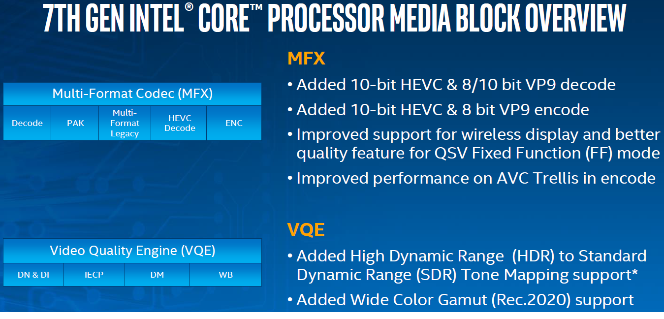
The Video Quality Engine also receives some tweaks for HDR and Wide Color Gamut (Rec.2020) support. Skylake’s VQE brought in RAW image processing support with a 16-bit image pipeline for selected filters. While Intel has not discussed the exact updates that enable Rec.2020 support, we suspect that more components in the VQE can now handle higher bit-widths. Intel pointed out that the HDR capabilities involve usage of both the VQE and the EUs in the GPU. So, there is still scope for further hardware acceleration and lower power consumption in this particular use-case.
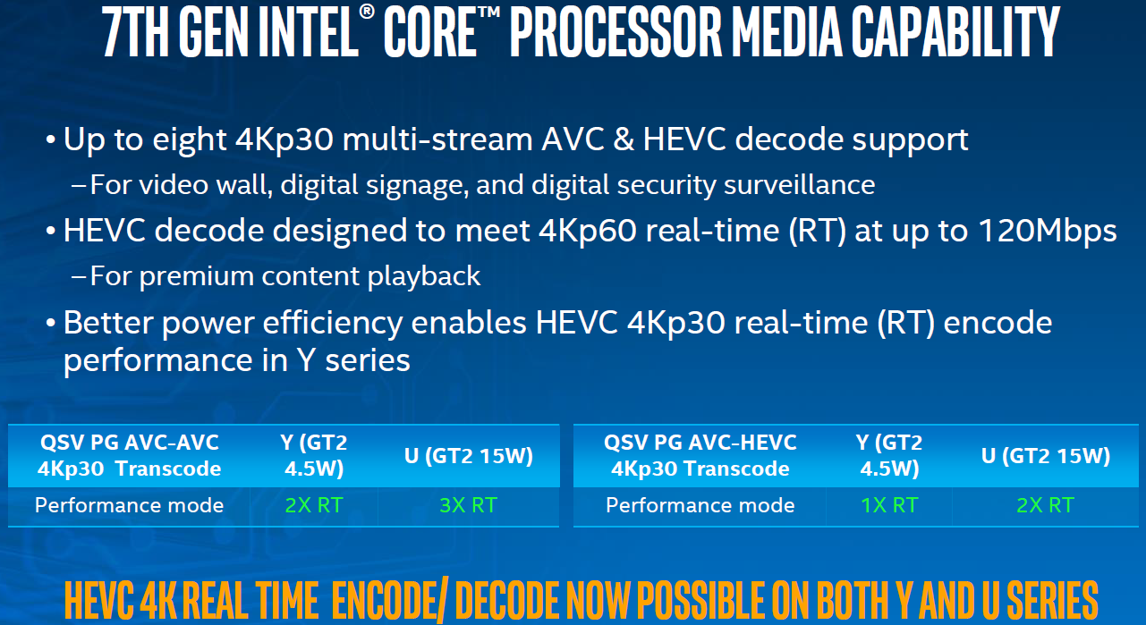
Intel claims that Kaby Lake-U/Y can handle up to eight 4Kp30 AVC and HEVC decodes simultaneously. HEVC decode support is rated at 4Kp60 up to 120 Mbps (especially helpful for premium content playback and Ultra HD Blu-ray). With Kaby Lake-U/Y’s process improvements, even the 4.5W TDP Y-series processors can handle real-time HEVC 4Kp30 encode.
On the subject of premium content, in their presentation Intel rather explicitly mentioned that the improved decode capabilities were, in part, for “premium content playback.” When we pushed Intel a bit on the matter – and specifically on 4K Netflix support – they didn’t have much to say beyond the fact that to play 4K Netflix, you need certification. Based on what was said and what was not said (and what we know about the certification process) our educated guess is that the updates in Kaby Lake-U/Y include some new DRM requirements for 4K content, and 4K Netflix should hopefully be good to go with the new platform. However on that note, because of those DRM requirements and that this is being pitched as a new feature for Kaby Lake, we suspect that when 4K Netflix streaming does come to the PC platform, Skylake owners are going to be out of luck.
It must be kept in mind that all the encode / decode aspects discussed above are for 4:2:0 streams. This is definitely acceptable for consumer applications, as even Blu-ray video streams (that have plenty of bandwidth at their disposal) are encoded in 4:2:0. However, if Intel wants to use the new media engine in professional broadcast and datacenter applications, 4:2:2, and, to a much lesser extent, even 4:4:4 support might become necessary. For the purpose of the Kaby Lake-U/Y consumer platforms being introduced today, this is not an issue at all.
Moving on, like the GPU core itself, Kaby Lake-U/Y’s display pipeline is the same as that of Skylake. This means the iGPU can support up to three simultaneous displays.

One of the disappointing aspects from Skylake that has still not been addressed in Kaby Lake-U/Y is the absence of a native HDMI 2.0 port with HDCP 2.2 support. Intel has been advocating the addition of an LSPCon (Level Shifter – Protocol Converter) in the DP 1.2 path. This approach has been used in multiple motherboards and even SFF PCs like the Intel Skull Canyon NUC (NUC6i7KYK) and the ASRock Beebox-S series. Hopefully, future iterations of Kaby Lake (such as the desktop and high-performance mobile parts coming in January) address this issue to simplify BOM cost for system vendors.
In summary, Kaby Lake-U/Y resolves one of the major complaints we had about Skylake’s media engine: the absence of hardware-accelerated 4Kp60 HEVC Main10 decode. There are a few other improvements under the hood that enable a more satisfying multimedia experience for consumers. The software and content-delivery ecosystems have plenty of catching up to do when it comes to taking full advantage of Kaby Lake-U/Y’s media capabilities.
One of the mysteries with the launch of Kaby Lake is the optimized 14nm+ process that Intel is promoting as one of the key components for the performance uptick in Kaby Lake. It’s worth noting that Intel has said nothing about caches, latencies or bandwidths. We are being told that the underlying microarchitecture for Kaby Lake is the same as Skylake, and that the frequency adjustments from the new process, along with features such as Speed Shift v2 and the new fixed function media codecs, account for the performance improvements as well as battery life increases when dealing with 4K content.
For users that speak in pure IPC, this may/may not be a shock. Without further detail, Intel is implying that Kaby Lake will have the same IPC as Skylake, however it will operate with a better power efficiency (same frequency at lower power, or higher frequency at same power) and for media consumption there will be more idle CPU cycles with lower power drain. The latter makes sense for mobile devices such as tablets, 2-in-1s and notebooks, or for power conscious users, but paints a static picture for the future of the desktop platform in January if the user only gets another 200-400 MHz in base frequencies.
However I digress with conjecture – the story not being told is on how has Intel changed its 14nm+ platform. We’ve only been given two pieces of information: taller fins and a wider gate pitch.
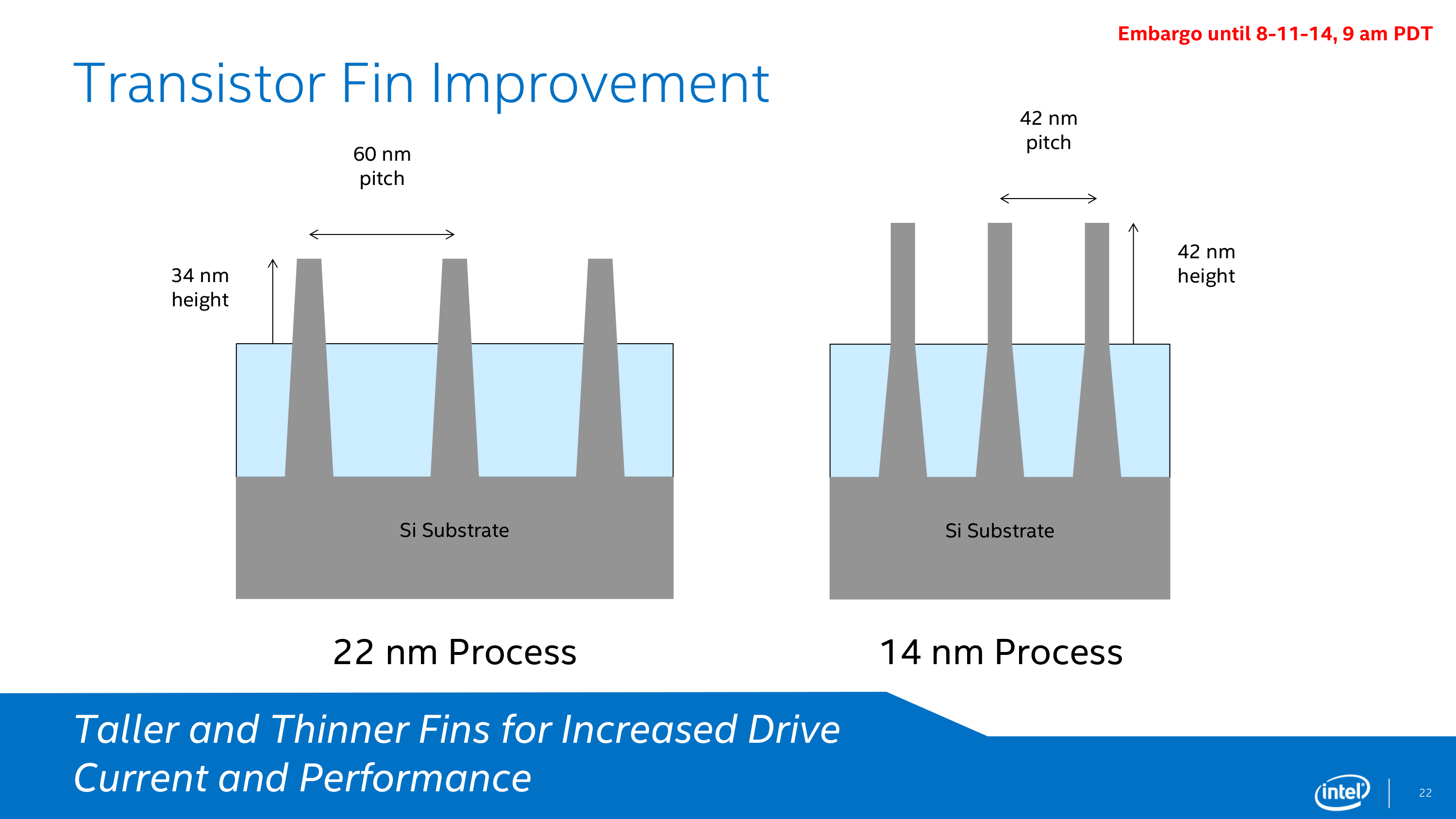
Intel 14nm Circa Broadwell
When Intel launched Broadwell on 14nm, we were given an expose into Intel’s latest and greatest semiconductor manufacturing lithography node. Intel at its core is a manufacturing company rather than a processor company, and by developing a mature and robust process node allows them to gain performance advantages over the other big players: TSMC, Samsung and GlobalFoundries. When 14nm was launched, we had details on their next generation of FinFET technology, discussions about the issues that faced 14nm as it was being developed, and fundamental dimensional data on how transistors/gates were proportioned. Something at the back of my brain says we’ll get something similar for 10nm when we are closer to launch.
But as expected, 14nm+ was given little extra detail. What would interest me is the scale of results or problems faced by the two changes in the process we know about. Taller fins means less driving current is needed and leakage becomes less of an issue, however a wider gate pitch is typically associated with a decrease in transistor density, requiring higher voltages but making the manufacturing process easier. There is also the argument that a wider pitch allows the heat generation of each transistor to spread more before affecting others, allowing a bit more wiggle room for frequency – this is at least how Intel puts it.
The combination of the two allows for more voltage range and higher frequencies, although it may come at the expense of die size. We are told that transistor density has not changed, but unless there’s a lot of spare unused silicon in the die for the wider pitch to spread, it seems questionable. It also depends which part of the metal stack is being adjusted as well. It’s worth noting that Intel has not released die size information at this time (we may get more exact numbers in January), and transistor counts as a metric is not being disclosed, similar to Skylake.
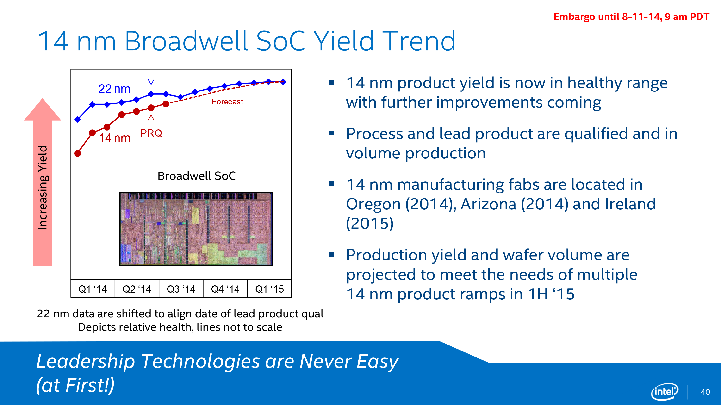
Finally, there’s some question over what it takes at a fab level to produce 14nm+. Though certainly not on the scale of making the jump to 14nm to begin with, Intel has been tight-lipped on whether any retooling is required. At a minimum, as this is a new process (in terms of design specificaitons), I think it’s reasonable to expect that some minor retooling is required to move a line over to 14nm+. In which case the question is raised over which Intel fabs can currently produce chips on the new process. One of the D1 fabs in Oregon is virtually guaranteed; whether Arizona or Ireland is also among these is not.
I bring this up because of the parallels between the Broadwell and Kaby Lake launches. Both are bottom-up launches, starting with the low wattage processors. In Broadwell’s case, 14nm yields – and consequently total volume – were a bottleneck to start with. Depending on the amount of retooling required and which fabs have been upgraded, I’m wondering whether the bottom-up launch of Kaby Lake is for similar reasons. Intel’s yields should be great even with a retooling, but if it’s just a D1 fab producing 14nm+, then it could be that Intel is volume constrained at launch and wants to focus on producing a larger number of small die 2+2 processors to start with, ramping up for larger dies like 4+2 and 4+4e later on.
Speed Shift v2
One of the new features for Skylake was Speed Shift. With the right OS driver, the system could relinquish control of CPU turbo to the CPU itself. Using internal metric collection combined with access to system-level sensors, the CPU could adjust the frequency with more granularity and faster than the OS can. The purpose of Speed Shift was to allow the system to respond quicker to requests for performance (such as interacting with a touch screen or browsing the web), reduce delays and improve the user experience. So while the OS was limited to predefined P-state options, a Speed Shift enabled processor with the right driver had a near contiguous selection of CPU multipliers within a wide range to select from.
The first iteration of Speed Shift reduced the time for the CPU to hit peak frequencies from ~100 milliseconds down to around 30. The only limitation was the OS driver, which is now a part of Windows 10 and comes by default. We extensively tested the effects of the first iteration of Speed Shift at launch.
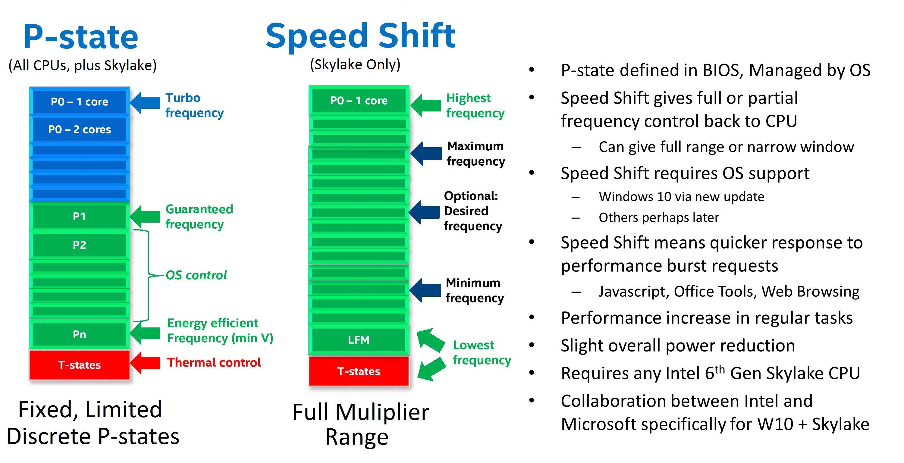
With Skylake, the hardware control around Speed Shift has improved. Intel isn’t technically giving this a new name, but it is an iterative updated which I prefer to call ‘v2’, if only because the adjustment from v1 to v2 is big enough to note. There is no change in the OS driver, so the same Speed Shift driver works for both v1 and v2, but the performance means that a CPU can now reach peak frequency in 10-15 milliseconds rather than 30.
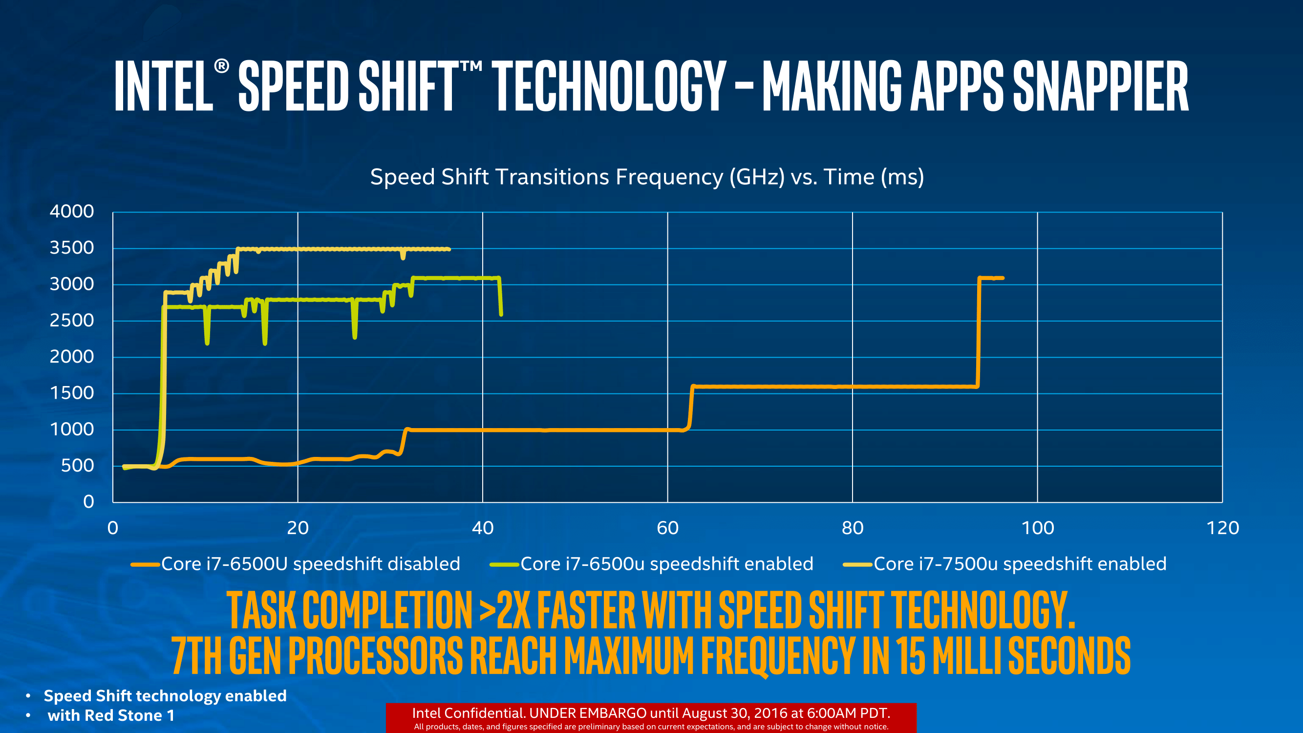
The green and yellow lines show the difference between v1 and v2, with the Core i7-7500U getting up to 3.5 GHz incredibly quickly. This will have an impact on latency limited interactions as well as situations where delays occur, such as asynchronous web page loading. Speed Shift is a play for user experience, so I’m glad to see it is being worked on. We will obviously have to test this when we can.
A note about the graph, to explain why the lines seem to zig-zag between lower and higher frequencies because I have encountered this issue in the past. Intel’s test, as far as we were told, relies on detecting register counters that increment as instructions are processed. By monitoring the value of these registers, the frequency can be extrapolated. Depending on the polling time, or adjacent point average (a common issue with counter based time benchmarks I’ve experienced academically), it can result it statistical variation depending on the capability of the code.
Performance
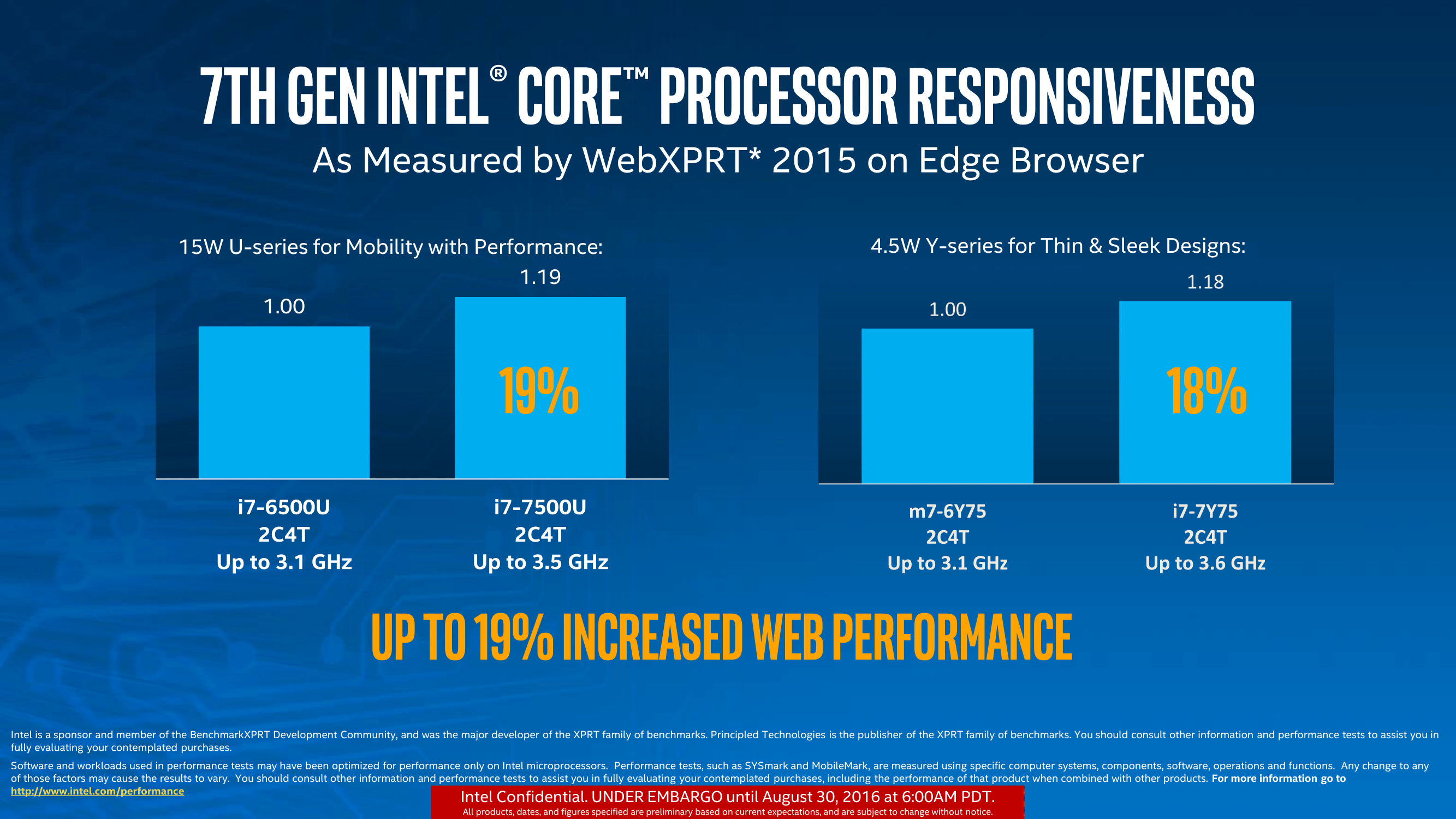
Similar to other performance claims made in the past couple of weeks, Intel was keen to show off how their new processors beat their old processors, as well as step over and above the really old stuff. Of course, benchmarks were selected that align with Intel’s regular development community, but Intel is claiming a 19% improvement in web performance over the previous generation:
Or a 12% performance uplift in general productivity taking into account various media/processing/data workloads provided by SYSMark:

For pure frequency adjustments, +400 MHz on 3.1 GHz is a 12.9% improvement, whereas +500 MHz on 3.1 GHz is a 16.1%. This accounts for most of the performance improvements for these tests, with WebXPRT extensively relying on short bursts of work to take advantage of Speed Shift v2 (WebXPRT was also a premium candidate for v1).
Perhaps a more important metric for improvement is how Intel has tackled 4K with their fixed function hardware. Moving the ability to encode/decode video from generic all-purpose hardware to fixed function allows the device to save CPU cycles but also save significant power. On a mobile device geared to consuming content, this translates as a direct improvement in battery life, assuming the display doesn’t decide to consume the excess. As we move to more efficient SoCs for video, but higher resolution displays, as long as the fixed function hardware keeps up with the content then the emphasis on battery life returns time and again to display efficiency.
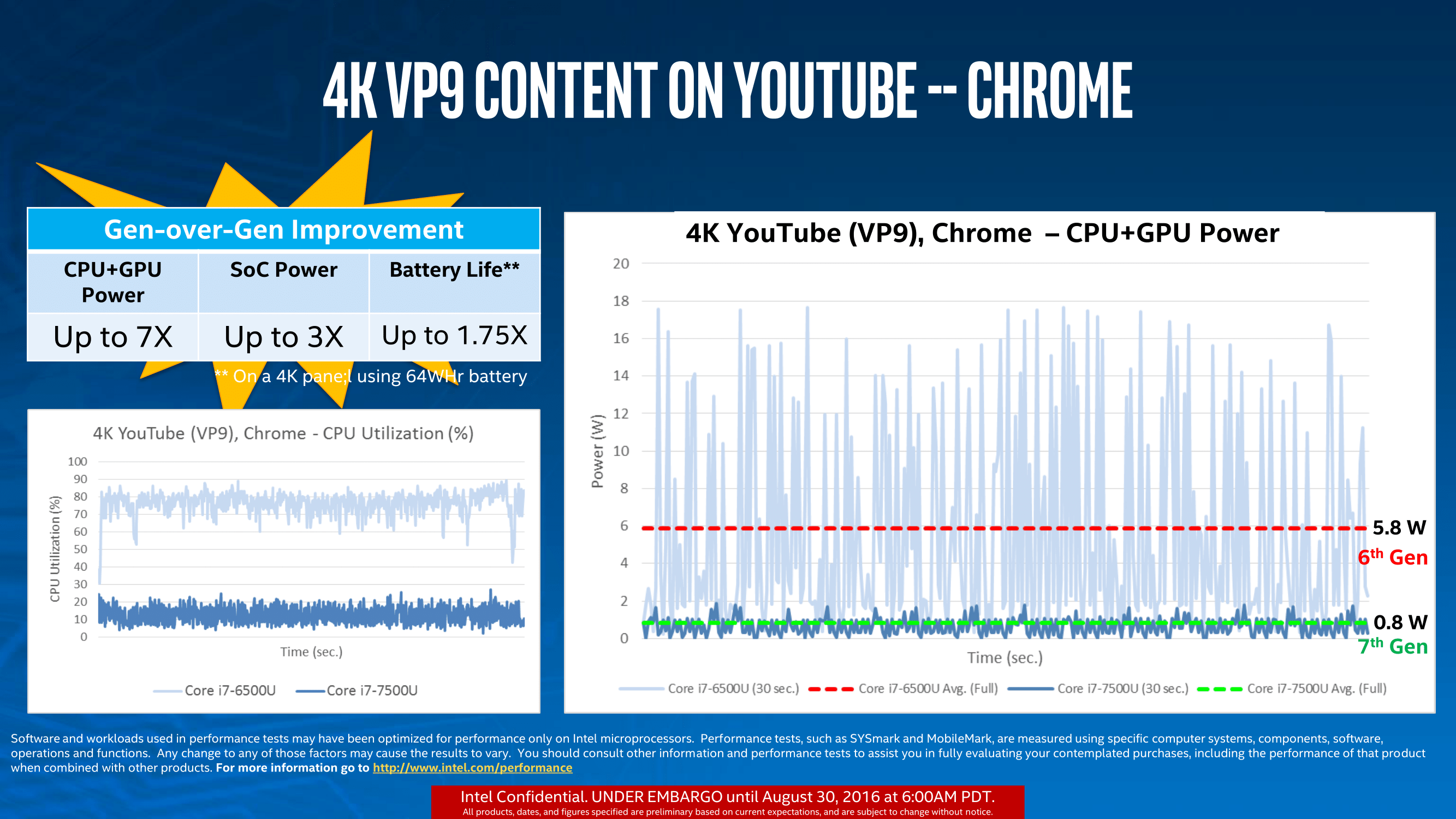
With that said, Intel provided two internal metrics for power consumption when consuming 4K video in 10-bit HEVC and 8-bit VP9.
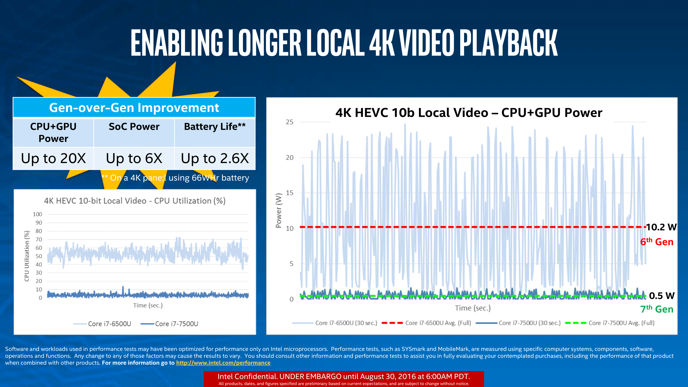
The key points for 10-bit HEVC at 4K are that CPU utilization is down to sub-5%, and system power consumption is reduced by a factor x20. Intel states that when using a 4K panel with a 66 Wh device, this translates into a 2.6x battery life improvement, or the ability to watch two films with ease.
Using VP9 is YouTube’s bread and butter, with more and more YouTube content being consumed every quarter. Depending on how your browser or settings forces which codec is played, with VP9 Intel states that CPU utilization reduces from 75-80% on the SKL-U part to under 20% on the KBL-U part. Again, this was tested by Intel as a 1.75x increase in battery life. One could argue that the prevalence of 4K recording hardware (smartphones) will make this important with more users creating content for many others to consume. However it should be noted that these improvements come when the integrated graphics are used – I’m sure we will see hardware with discrete graphics in play and it will be up to the firmware to decide to use either the new fixed function parts or to engage the discrete card.
Takeaway Performance Message
On the whole, Kaby Lake comes with the following performance breakdown:
- Same IPC as Skylake, but better manufacturing gives 12-16% more frequency
- Speed Shift v2 will improve latency focused metrics, such as user experience
- New fixed function hardware for 4K HEVC/VP9 increases battery life for media consumption
- OPI 3.0 enables support for PCIe 3.0 x4 NVMe drives and Thunderbolt 3 (with additional controllers)
- Support for three 4K displays: DP 1.2, HDMI 1.4, eDP 1.2
Calling back to Computex, ASUS first announced a new Transformer device based on ‘Intel’s Next Generation’ processor. We knew it was Kaby Lake, but given the launch cycle for KBL it was understandable that the device was still a couple of months out and a work in process. At that point of the game the hardware specifications are typically squared away, and final touches are being made to the design ID as well as strong work on the software platform and ramping up the manufacturing aspect. We expect ASUS to launch their new Transformer products in due course.

At Intel’s pre-briefing for Kaby Lake, several systems were on display from HP all using the new processors. Specifications were not discussed, however devices with 4K panels and a variety of sizes were shown, including what looked like an upgraded Spectre, as well as a notebook with an OLED display.


This week is the annual IFA trade show in Berlin, which focuses on complete consumer electronics rather than components, as well as home appliances, IoT, and other things in-between. We have presentations and press events for a wide variety of companies including Acer, Samsung, Lenovo, Huawei, ZTE, and Sony, all of whom could be announcing something around Kaby Lake. (Qualcomm and AMD are also presenting at the show, but something tells me it isn’t to do with KBL.)
Explaining Why There’s No Desktop Parts Today
For the majority of enthusiasts, PC builders and gamers, questions about the time frame of the desktop processor launches, the benefits they bring and the pricing are swirling around the zeitgeist. Intel has confirmed with today’s launch that a wider array of Kaby Lake parts will be launched in January, including Iris graphics enabled processors, desktop parts, enterprise parts and workstation SKUs (vPro and Xeons, one would assume).
Despite the fact that this is still 14nm, one could assume that 14nm+ was focused on the small die parts first to improve yield before the larger desktop parts were produced, depending on how difficult the shift from 14 to 14+ actually was. There’s also the consideration about Intel’s product lines: Skylake on the desktop was only launched 12 months ago, and the next generation 10nm Intel product is – admittedly looking into a very foggy crystal ball – over a year away and will be mobile focused again as smaller dies are easier to make. Intel has to sufficiently space out its product stacks to ensure maximum profit, appease shareholders, but also give their customers a regular, expected update cycle. There’s a reason we don’t see the best product Intel could ever make on day one at unlimited expense.
Given that Intel has said that KBL is a similar IPC to SKL, it might be a bit worrying if desktop performance of the new parts is identical to the old ones, merely bumped up in frequency. Typically a small frequency bump mirrors a basic overclock; importantly however, if the pitch has been widened to allow a higher frequency, this could have a beneficial knock on effect for overclocking. Despite marketing efforts, Intel still limits overclocking to the two high-end SKUs, so how well Kaby Lake overclocks could prove important with desktop enthusiasts. If it overclocks better than Skylake, then we might be looking at the Skylake equivalent of the Haswell Refresh/Devil’s Canyon. However if KBL offers the same OC frequency as SKL, and the same performance due to a similar IPC, then enthusiasts might not be interested. Ultimately Intel is going to market the new chips as a 3-5 year upgrade option for users still on Nehalem, Westmere and Sandy Bridge. This is ultimately where Intel believes most of the upgrade sales are coming from, rather than users jumping from Skylake.
The other factor is the motherboard side of the equation. We know that Kaby Lake on the desktop is to be accompanied by a new chipset launch as well, the 200-series, and typically if we were expecting a September launch then we would have seen motherboard examples at Computex. At the show, only MSI had an ‘unlabeled 200-series’ motherboard on show, which looked pretty identical to a Z170 product already on sale barring the design ID. We don’t yet know the benefits of the 200-series chipset over the 100-series line, and a release date in January would mean that motherboard manufacturers should now be in the final design steps for their major SKUs.
Saying ‘January’ as a launch date is quite vague. But, January has the annual CES event in Las Vegas during the first week after New Year, which is a common time to launch new CPUs after the holiday season finishes and people are ‘rested’.
Finally, it’s also worth noting that AMD is planning to enable widespread availability for their new Zen set of CPUs in Q1. So a January launch for desktop Kaby Lake could provide a more contested one for Intel. (If they also launch at CES, I need to start bulk ordering caffeine drips today. Goodbye sleep, it was nice knowing you. I may not be seen the rest of January.)
After all that, I’m pretty sure it’s pronounced Kay-bee Lake.


Autore: AnandTech