
Author: AnandTech

Intel this morning is lifting the lid on some of the finer architectural and technical details about its upcoming Lunar Lake SoC – the chip that will be the next generation of Core Ultra mobile processors. Once again holding one of their increasingly regular Tech Tour events for media and analysts, Intel this time set up shop in Taipei just before the beginning of Computex 2024. During the Tech Tour, Intel disclosed numerous facets of Lunar Lake, including their new P-Core design codenamed Lion Cove and a new wave of E-cores that are a bit more like Meteor Lake’s pioneering Low Power Island E-Cores. Also disclosed was the Intel NPU 4, which Intel claims delivers up to 48 TOPS, surpassing Microsoft’s Copilot+ requirements for the new age of AI PCs.
Intel’s Lunar Lake represents a strategic evolution in their mobile SoC lineup, building on their Meteor Lake launch last year, focusing on enhancing power efficiency and optimizing performance across the board. Lunar Lake dynamically allocates tasks to efficient cores (E-cores) or performance cores (P-cores) based on workload demands by leveraging advanced scheduling mechanisms, which are assigned to ensure optimal power usage and performance. Still, once again, Intel Thread Director, along with Windows 11, plays a pivotal role in this process, guiding the OS scheduler to make real-time adjustments that balance efficiency with computational power depending on the intensity of the workload.
Intel CPU Architecture Generations
Alder/Raptor Lake
Meteor
Lake
Lunar
Lake
Arrow
Lake
Panther
Lake
P-Core Architecture
Golden Cove/
Raptor Cove
Redwood Cove
Lion Cove
Lion Cove
Cougar Cove?
E-Core Architecture
Gracemont
Crestmont
Skymont
Crestmont?
Darkmont?
GPU Architecture
Xe-LP
Xe-LPG
Xe2
Xe2?
?
NPU Architecture
N/A
NPU 3720
NPU 4
?
?
Active Tiles
1 (Monolithic)
4
2
4?
?
Manufacturing Processes
Intel 7
Intel 4 + TSMC N6 + TSMC N5
TSMC N3B + TSMC N6
Intel 20A + More
Intel 18A
Segment
Mobile + Desktop
Mobile
LP Mobile
HP Mobile + Desktop
Mobile?
Release Date (OEM)
Q4’2021
Q4’2023
Q3’2024
Q4’2024
2025
Lunar Lake: Designed By Intel, Built By TSMC (& Assembled By Intel)
While there are many aspects of Lunar Lake to dive into, perhaps it’s best we start with what’s sure to be the most eye-catching: who’s building it.
Intel’s Lunar Lake tiles are not being fabbed using any of their own foundry facilities – a sharp departure from historical precedence, and even the recent Meteor Lake, where the compute tile was made using the Intel 4 process. Instead, both tiles of the disaggregated Lunar Lake are being fabbed over at TSMC, using a mix of TSMC’s N3B and N6 processes. In 2021 Intel set about freeing their chip design groups to use the best foundry they could – be it internal or external – and there’s no place that’s more apparent than here.
Overall, Lunar Lake represents their second generation of disaggregated SoC architecture for the mobile market, replacing the Meteor Lake architecture in the lower-end space. At this time, Intel has disclosed that it uses a 4P+4E (8 core) design, with hyper-threading/SMT disabled, so the total thread count supported by the processor is simply the number of CPU cores, e.g., 4P+4E/8T.

The build-up of Lunar Lake combines a synergetic collaboration between Intel’s architectural design team and TSMC’s manufacturing process nodes to bring the latest Lion Cove P-cores to Lunar Lake, which boosts Intel’s architectural IPC as you would expect from a new generation. At the same time, Intel also introduces the Skymont E-cores, which replace the Low Power Island Cresmont E-cores of Meteor Lake. Notably, however, these E-cores don’t connect to the ring bus like the P-cores, which makes them a sort of hybrid LP E-core, combining the efficiency gains of the more advanced TSMC N3B node with the double-digit gains in IPC over the previous Crestmont cores.
The entire compute tile, including the P and E-cores, is built on TSMC’s N3B node, while the SoC tile is made using the TSMC N6 node.
At a higher level, Intel is once again using their Foveros packaging technology here. Both the compute and SoC (now the “Platform Controller”) tiles sit on top of a base tile, which provides high-speed/low-power routing between the tiles, and further connectivity to the rest of the chip and beyond.
In another first for a mainstream Intel Core product, the Lunar Lake SoC platform also includes up to 32 GB of LPDDR5X memory on the chip package itself. This is arranged as a pair of 64-bit memory chips, offering a total 128-bit memory interface. As with other vendors using on-package memory, this change means that users can’t just upgrade DRAM at-will, and the memory configurations for Lunar Lake will ultimately be determined by what SKUs Intel opts to ship.

With Lunar Lake, Intel is also strongly focusing on AI, as the architecture integrates a new NPU called NPU 4. This NPU is rated for up to 48 TOPS of INT8 performance, thus making it Microsoft Copilot+ AI PC ready. This is the bar all of the PC SoC vendors are aiming for, including AMD and Qualcomm too.
Intel’s integrated GPU will also be a contributing player here. While not the highly efficient machine that the dedicated NPU is, the Arc Xe2-LPG brings dozens of additional T(FL)OPS of performance with it, and some additional flexibility an NPU doesn’t come with. Which is why you’ll also see Intel rating the performance of these chips in terms of total platform TOPS – in this case, 120 TOPS.
Intel’s collaboration with Microsoft further enhances workload management through the fabled Intel Thread Director, optimized for applications such as the Copilot assistant. Given the time of the introduction of Lunar Lake, it somewhat sets the stage for a Q3 2024 launch, which coincides with the holiday 2024 market.
Intel Lunar Lake: Updating Intel Thread Director & Power Management Improvements
To say that energy efficiency is a key goal for Lunar Lake would be an understatement. For as much as Intel is riding high in the mobile PC CPU market (AMD’s share there is still but a fraction), the company has been feeling the pressure over the last few years from customer-turned-rival Apple, whose M-series Apple Silicon has been setting the bar for power efficiency over the last few years. And now with Qualcomm attempting to do the same things for the Windows ecosystem with their forthcoming Snapdragon X chips, Intel is preparing to make their own power play.
Intel’s Thread Director and power management updates for Lunar Lake show various and significant improvements compared to Meteor Lake. The Thread Director uses a heterogeneous scheduling policy, initially assigning tasks to a single E-core and expanding to other E-cores or P-cores as and when needed. OS containment zones are designed to limit tasks to specific cores, which directly improves power efficiency and delivers the performance needed by the right core for the workload at hand. Integration with power management systems and a quad array of Power Management Controllers (PMC) further allows the chip, in concert with Windows 11, to make context-aware adjustments, ensuring optimal performance with minimal power usage and wastage.

Lunar Lake’s scheduling strategy effectively handles power-sensitive applications. One example Intel gave is that video conferencing tasks are kept within the efficiency core cluster, utilizing the E-cores to maintain performance while reducing power consumption by up to 35%, as shown by Intel’s provided data. These improvements are achieved through collaboration with OS developers such as Microsoft for seamless integration for optimizing for the best balance between power consumption and performance.

Focusing on the power management system for Lunar Lake, Intel uses its SoC power management, operating in efficiency, balance, and performance modes tailored and designed to adapt to whatever the demands of the workload at the time of operation. This multi-layered approach allows the Lunar Lake SoC to operate efficiently. Again, much like the Intel Thread Director, the PMCs can balance power usage with performance needs.

Intel further plans to enhance the Thread Director by increasing scenario granularity, implementing AI-based scheduling hints, and enabling cross-IP scheduling within Windows 11. These enhancements essentially equate to workload management designed to boost overall power efficiency and deliver performance across various applications when needed without wasting power budget by allocating lighter tasks to the higher power P-cores.
Over the next few pages, we’ll explore the new P and E cores and Intel’s update to ther integrated Arc Xe (Xe2-LPG) graphics.
The Intel Lion Cove CPU architecture brings with it some changes to improve the performance and efficiency of Intel’s P-cores.
Key among these improvements is a significant overhaul of Intel’s traditional P-core cache hierarchy. The fresh design for Lion Cove uses a multi-tier data cache containing a 48KB L0D cache with 4-cycle load-to-use latency, a 192KB L1D cache with 9-cycle latency, and an extended L2 cache that gets up to 3MB with 17-cycle latency. In total, this puts 240KB of cache within 9 cycles’ latency of the CPU cores, whereas Redwood Cove before it could only reach 48KB of cache in the same period of time.
The data translation lookaside buffer (DTLB) has also been revised, increasing its depth from 96 to 128 pages in order to improve its hit rate.

Lastly, Intel has added a third Address Generation Unit (AGU)/Store Unit pair to further boost store performance. Notably, this brings the number of load and store pipelines into balance at 3 each; in most Intel architectures, there have been more load units than store units.
Overall, in true long-term CPU design fashion, Intel has thrown more cache at the problem. As CPU complexity grows, so do the cache subsystems to keep them fed. In this case, keeping the lion fed is a key improvement in improving its performance as well as keeping up its power efficiency.
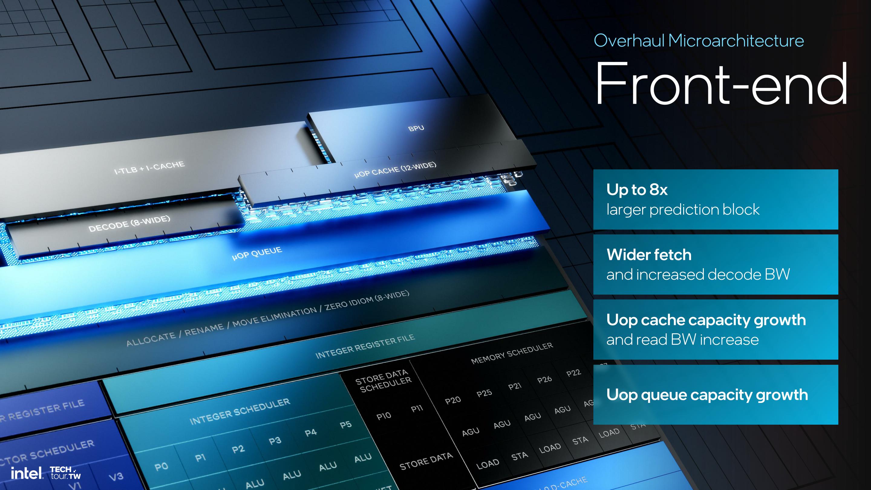
Diving into the compute architecture of Lion Cove, the architecture takes another step forward with Intel’s P-core designs, again with a focus on delivering performance and efficiency improvements. The architecture has a new front-end approach to processing an instruction with a prediction block 8x larger, broader fetch, higher decode bandwidth, and an enormous growth in Uops cache capacity and reads bandwidth. The UOP queue capacity is increased, which also improves the overall throughput. In execution, the out-of-order engine of Lion Cove is partitioned between an Integer (INT) and a Vector (VEC) domain, which has independent renaming and scheduling capabilities.

This type of partitioning allows for expandability in the future, independent growth of each domain, and benefits toward reduced power consumption for a domain-specific workload. The out-of-order engine is also improved, going from 6 to 8-wide allocation/rename and 8 to 12-wide retirement, with the deep instruction window increased from 512 to 576 entries and from 12 to 18 execution ports. These changes make the pipeline more robust and more flexible for execution.
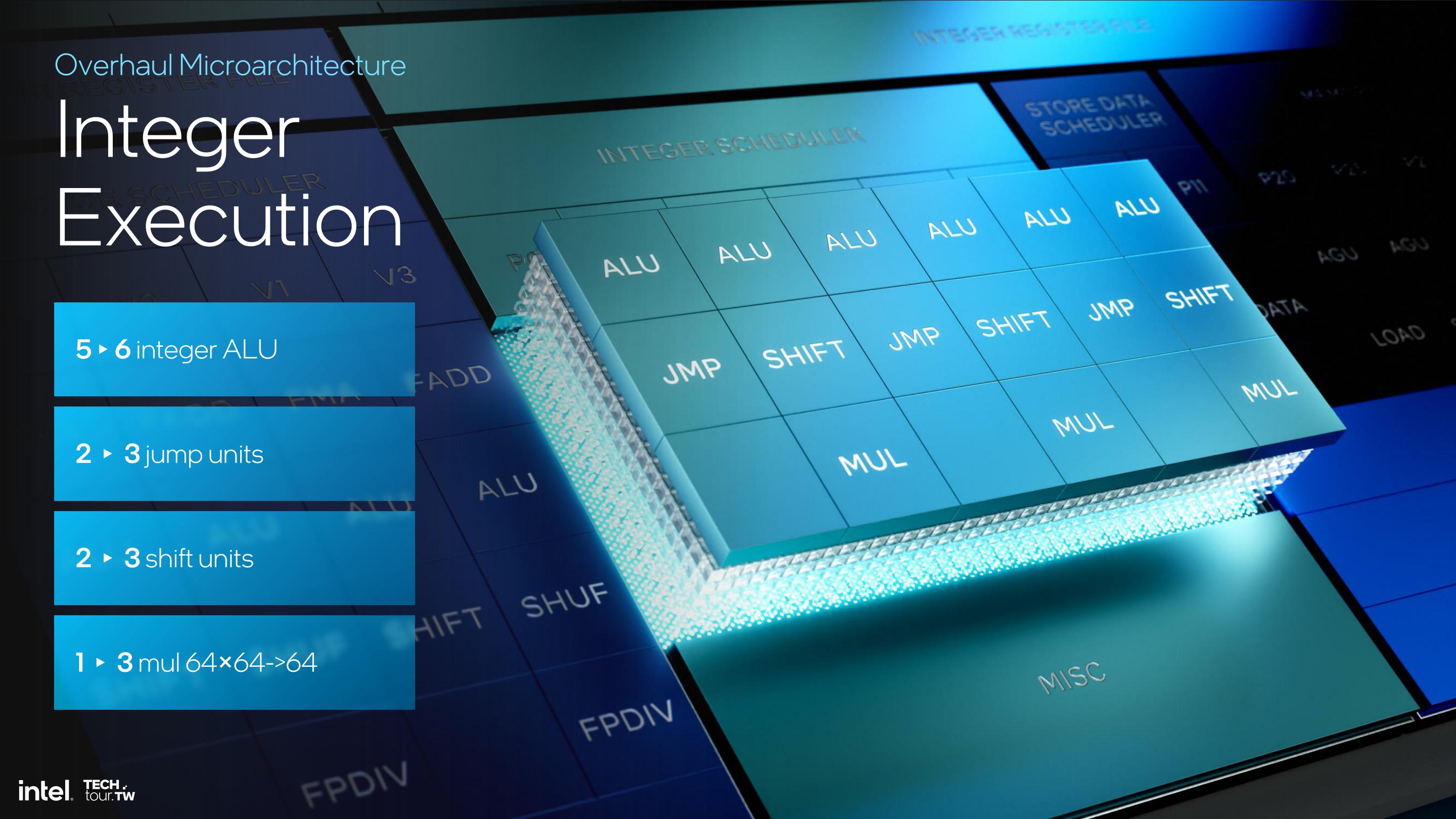
The integer execution units in Lion Cove are also improved, with increased units from 5 to 6 integer ALUs, 2 to 3 jump units, and 2 to 3 shift units. They multiply units from 64×64 to 64, increasing from 1 to 3, providing even more computing power for the most complex operations. Another striking advance is the migration in the P-core database from a ‘sea of fubs’ to a ‘sea of cells’. This process of updating the organization of the P-cores substructure moves from tiny, latch-dominated partitions to more extensive and ever larger flop-dominated partitions that are very agnostic as things go.

This Lion Cove architecture also aligns with performance increases, boasting a predicted double-digit bump in IPC over the older Redwood Cove generation. This uplift is noticed, especially in the betterment of its hyper-threading, whereby improved IPC by 30%, dynamic power efficiency improved by 20%, and previous technologies, in balancing, without increasing the core area, in a commitment of Intel to better performance, within existing physical constraints.
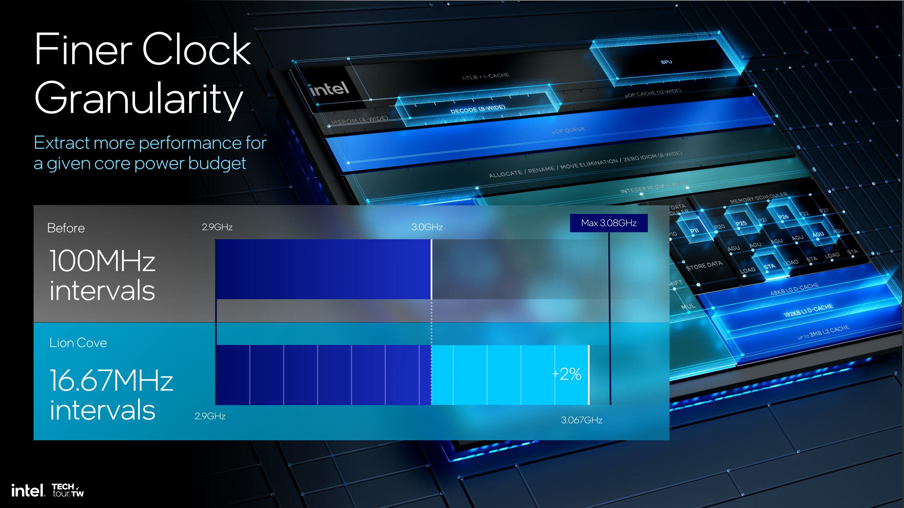
Power management has also been refined by including AI self-tuning controllers to replace the static thermal guard-bands. It lets the system respond dynamically to the actual real-time operating conditions in an adaptive way to achieve higher sustained performance. It uses a finer clock granularity, now making the 16.67MHz intervals. Rather than 100MHz, this means more accurate power management and performance tuning for maximum efficiency from the power budget.
At least on paper, Lion Cove looks to be a nice upgrade over Golden Cove. It incorporates improved memory and cache subsystems, better power management, and an increase in IPC performance without concentrating on boosting for faster frequencies.
The Skymont E-cores, designed for a new level of efficiency and performance, are at the heart of Intel’s Lunar Lake architecture.
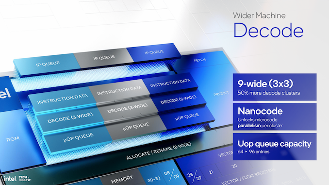
Skymont cores feature a significantly more comprehensive machine architecture, starting with a 9-wide decode stage that includes 50% more decode clusters than previous generations. This is supported by a larger micro-op queue, which now holds 96 entries compared to 64 in the older design. Using “Nanocode” adds further microcode parallelism within each decode cluster.

Significant improvements have also been made in the out-of-order execution engine. The allocation width has been increased to 8 wide, while the retirement stage has been doubled to 16 wide. This enhances the core’s ability to issue and execute multiple instructions simultaneously and reduces latency through dependency-breaking mechanisms.

Skymont deepens the reorder buffer to 416 entries compared to the previous 256 regarding queuing and buffering capabilities. Additionally, the sizes of the physical register files (PRF) and reservation stations have been increased. These enhancements allow the core to handle many more instructions in flight, thereby increasing parallelism in instruction execution.
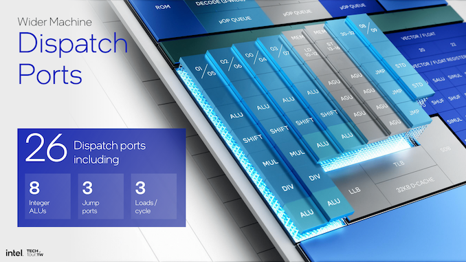
Note that dispatch ports initially became 26, with 8 for integer ALUs, 3 for jump operations, and 3 for load operations per cycle, further allowing flexible and efficient resource allocation. In vector performance, Skymont supports 4×128-bit FP and SIMD vectors, which doubles gigaflops/TOPs and reduces latency for floating-point operations. The company has also redesigned the memory subsystem, with a 4MB L2 cache shared among four cores, doubling the L2 bandwidth to 128B per cycle, and in the process, reduces memory access latencies while improving data throughput.

Performance metrics highlight sizeable gains in power efficiency: single-threaded performance increases by 1.7X while consuming just one-third of the power relative to Meteor Lake’s LP E-cores.

Multi-threaded performance is 2.9X faster with the same power reduction across the board when comparing the Skymont E-core cluster directly to Meteor Lake and its LP E-core.
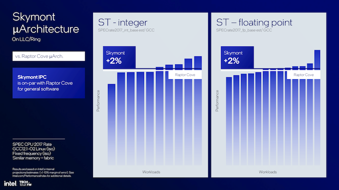
That’s equally useful for mobile and desktop designs. In other words, Skymont E-cores are very flexible, with due leverage given to low-power fabric and system cache for mobile scenarios and multi-threaded throughput optimized for desktop compute tiles. Compared to Raptor Cove, Skymont offers 2% better integer and floating-point performance in single-threaded workloads, with a power and thermal envelope almost identical to its predecessor’s.
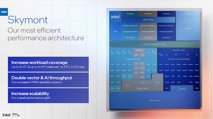
In this way, E-cores for Skymont represent the next step in Intel’s architectural development, creating a marked improvement in decoding, execution, memory subsystems, and power efficiency in meeting the needs of more power-efficient compute, as well as optimizing for improved IPC gains over the previous Crestmont E-cores.
Perhaps Intel’s main focal point, from a marketing point of view, is the latest generational change to its Neural Processing Unit or NPU.Intel has made some significant breakthroughs with its latest NPU, aptly called NPU 4. Although AMD disclosed a faster NPU during their Computex keynote, Intel claims up to 48 TOPS of peak AI performance.NPU 4, compared with the previous model, NPU 3, is a giant leap in enhancing power and efficiency in neural processing. The improvements in NPU 4 have been made possible by achieving higher frequencies, better power architectures, and a higher number of engines, thus giving it better performance and efficiency.

In NPU 4, these improvements are enhanced in vector performance architecture, with higher numbers of compute tiles and better optimality in matrix computations.This incurs a great deal of neural processing bandwidth; in other words, it is critical for applications that demand ultra-high-speed data processing and real-time inference. The architecture supports INT8 and FP16 precisions, with a maximum of 2048 MAC (multiply-accumulate) operations per cycle for INT8 and 1024 MAC operations for FP16, clearly showing a significant increase in computational efficiency.

A more in-depth look at the architecture reveals increased layering in the NPU 4. Each of the neural compute engines in this 4th version has an incredibly excellent inference pipeline embedded — comprising MAC arrays and many dedicated DSPs for different types of computing. The pipeline is built for numerous parallel operations, thus enhancing performance and efficiency. The new SHAVE DSP is optimized to four times the vector compute power it had in the previous generation, enabling more complex neural networks to be processed.

A significant improvement of NPU 4 is an increase in clock speed and introducing a new node that doubles the performance at the same power level as NPU 3. This results in peak performance quadrupling, making NPU 4 a powerhouse for demanding AI applications. The new MAC array features advanced data conversion capabilities on a chip, which allow for a datatype conversion on the fly, fused operations, and layout of the output data to make the data flow optimal with minimal latency.

The bandwidth improvements in NPU 4 are essential to handle bigger models and data sets, especially in transformer language model-based applications. The architecture supports higher data flow, thus reducing the bottleneck and ensuring it runs smoothly even when in operation. The DMA (Direct Memory Access) engine of NPU 4 doubles the DMA bandwidth—an essential addition in improving network performance and an effective handler of heavy neural network models. More functions, including embedding tokenization, are further supported, expanding the potential of what NPU 4 can do.
The significant improvement of NPU 4 is in the matrix multiplication and convolutional operations, whereby the MAC array can process up to 2048 MAC operations in a single cycle for INT8 and 1024 for FP16. This, in turn, makes an NPU capable of processing much more complex neural network calculations at a higher speed and lower power. That makes a difference in the dimension of the vector register file; NPU 4 is 512-bit wide. This implies that in one clock cycle, more vector operations can be done; this, in turn, carries on the efficiency of the calculations.

NPU 4 supports activation functions and a wider variety is available now that supports and treats any neural network, with the choice of precision to support the floating-point calculations, which should make the computations more precise and reliable. Improved activation functions and an optimized pipeline for inference will empower it to do more complicated and nuanced neuro-network models with much better speed and accuracy.

Upgrading to SHAVE DSP within NPU 4, with four times the vector compute power compared to NPU 3, will bring a 12x overall increase in vector performance. This would be most useful for transformer and large language model (LLM) performance, making it more prompt and energy efficient. Increasing vector operations per clock cycle enables the larger vector register file size, which significantly boosts the computation capabilities of NPU 4.
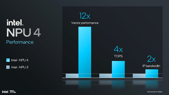
In general, NPU 4 presents a big performance jump over NPU 3, with 12 times vector performance, four times TOPS, and two times IP bandwidth. These improvements make NPU 4 a high-performing and efficient fit for up-to-date AI and machine learning applications where performance and latency are critical. These architectural improvements, along with steps in data conversion and bandwidth improvements, make NPU 4 the top-of-the-line solution for managing very demanding AI workloads.
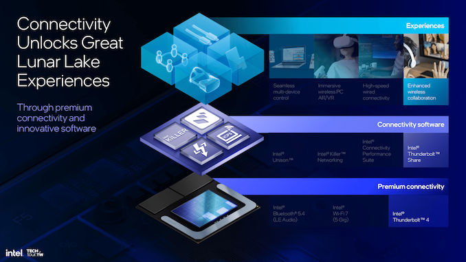
Intel’s recent in-road developments in I/O and connectivity with the Lunar Lake platform translate into big leaps ahead of Meteor Lake in what’s available in terms of performance and efficiency. Key highlights for Lunar Lake include native Thunderbolt 4 connectivity, the new Thunderbolt Share functionality, and the upgrade to Wi-Fi 7 wireless connectivity.

Thunderbolt 4 builds excellently on the foundation laid by Thunderbolt 3, which isn’t new from a controller standpoint, but it does offer enhancements in connectivity and bandwidth, and being internally opted for is the key difference here. The fact that three Thunderbolt ports are now allowed for every laptop makes this feature very flexible and usable.
Another improvement with Thunderbolt 5 SSDs is the 25% upgrade in read and write speeds, which increases the overall data transfer rate and reduces the time it takes to transfer files. This is important for applications that require high data transfer rates, like video editing and working on files of considerable size, so users do not lag or lag at minimal rates in their work.

Thunderbolt Share is a new technology within Lunar Lake. It allows multiple PCs to share screens, monitors, keyboards, mice, and storage across systems in a straightforward and fast manner at up to 60 frames per second.

Specifically, this is very important in collaborative environments whereby sharing data is made easy and quick, thus improving workflow. The utility in productivity tasks allows users to sync folders and has a drag-and-drop file sharing function between PCs at high speeds.

Wi-Fi 7 is also integrated into the Lunar Lake platform, which Meteor Lake omitted in terms of wireless connectivity. This multi-link operation feature of Wi-Fi 7 adds wireless signal integrity and reliability and increases throughput with less latency by duplicating packets across all links above. This implies smoother performance and better load balancing, even in demanding applications. The greatest benefit from Wi-Fi 7’s new capabilities comes to the user when dealing with bandwidth-intensive tasks; it is designed to allow users a stable and effective wireless connection.

It also includes RF Interference Mitigation technology, where the DDR clock frequency is automatically tuned to minimize interference with Wi-Fi signals. This function saves 50% of throughput degradation caused by memory noise; thus, theoretically, it should uplift the performance of the entire wireless network. Another positive effect users can expect is robust connectivity, even in very demanding environments.

Intel’s partnership with Meta goes further, tapping into this Wi-Fi 7 technology to enhance VR experiences. This further optimizes the video latency performance and reduces interference, thus making VR applications more seamless and engaging, at least from a wireless connectivity viewpoint. The new enhancements of Wi-Fi 7 offer high, reliable speed with low latency to meet the most challenging needs in VR applications.
Altogether, Intel’s platform on Lunar Lake with Thunderbolt 4, Thunderbolt Share, and Wi-Fi 7 represents an all-around upgrade in connectivity solutions compared to Meteor Lake. These technologies bring enhancements across the board, including massive data swapping that takes place, with gains in speed and reliability in both wired and wireless connectivity, with the aim of extending and improving the end-user experience.
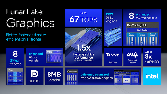
Along with Lunar Lake, Intel has just unveiled its Xe2 graphics architecture for mobile, supported by the 2nd Generation Arc Xe Core. On paper, it offers an extraordinary bump in performance and efficiency. Aside from gaming, which we don’t think the 4P+4E part would cut it, we’ve opted to focus on the critical takeaways of Intel’s presentation for graphics, including the media engine within.

Intel’s introduction of the Xe2 architecture significantly improves computational capabilities by providing up to 67 TOPs and offering increased ray tracing units compared to Xe-LPG on Meteor Lake. According to Intel, the 2nd gen Xe-cores offer 1.5x faster graphics performance than Meteor Lake, which is helped and achieved by the new XMX engines. Enhanced XeSS kernels deliver improved graphics and compute performance.

One element that Intel looks to have changed from Meteor Lake is that it offers more flexible and higher-quality display outputs. Within the Display engine, the streams in the dual-pixel pipeline can be combined for multi-stream transport. With this architecture, ports will be available in four locations, which will be flexible for connectivity. An eDP port is also provided in Intel’s configuration, which will augment the display to set high resolutions and refresh rates for the output on high-end, premium, and capable displays.

Intel’s eDisplayPort 1.5 includes the panel replay feature integrated with adaptive sync and selective update mechanisms. This helps decrease power consumption by refreshing only the parts of the screen that change instead of the entire display. These innovations save not only energy but also improve visual experiences by reducing display lag and increasing sync precision.

Portraying the pixel processing pipeline is one of the fundamental bases on which Intel’s display engine sits, enabling six planes per pipeline for advanced color conversions and compositions. In addition, it integrates hardware support for color enhancement, display scaling, pixel tuning, and HDR perceptual quantization, ensuring that the graphics on the screen is vibrant and accurate. The design is quite flexible, highly power-efficient, and performance-engineered to support various input and output formats, at least on paper. Intel hasn’t provided any quantifiable power metrics, TDPs, or other power elements so far.

When considering compression and encoding, the architecture Xe2 extends up to 3:1 display stream compression visually losslessly, including transport encoding for HDMI and DisplayPort protocols. These chip features further reduce the data load and maintain high resolution at the output without losing visual quality.

Intel’s adoption of the VVC codec is a big deal for video compression technology improvement. This codec offers up to a 10% reduction in file size compared to AV1, supported by adaptive resolution streaming and advanced content coding for 360-degree and panoramic videos. This will ensure lower bitrates for streaming without losing quality—an essential aspect for modern multimedia applications.

The Windows GPU software stack is robust, from top to bottom, with the support of D3D, Vulkan, and Intel VPL APIs and frameworks. This means that combining these qualities provides comprehensive support for the varied runtimes and drivers in the market, thus increasing its overall efficiency and compatibility in different software climates.
Intel’s Xe2 and second-generation Arc Xe Core improve performance, efficiency, and flexibility significantly. These innovations strengthen Intel’s position in the competitive landscape of solutions for mobile graphics, with reinforced capabilities across display, media, and compute operations.
So, what’s Lunar Lake all about? We know that Lunar Lake isn’t built using any of Intel’s nodes, which may come as a massive surprise to some, but it does leverage TSMC’s 3 nm N3B node, and on paper, it looks like a significant upgrade to Meteor Lake. Lunar Lake seems like a big mobile CPU architectural uplift from Intel when compared directly to Meteor Lake in the mobile SoC space, marking a big jump in task-specific processing capabilities. Now, they integrated Lion Cove P-cores with Skymont E-cores, addressing the intensive task together with the background activities to ensure maximum performance. #
Also, the inclusion of NPU 4, which pumps 48 TOPS, makes Lunar Lake a strong competitor in the AI and machine learning field, with “world-class” AI performance, highlighting Intel’s investment in AI for the AI-driven future. However, AMD’s recent Zen 5 and Ryzen AI 300-based disclosure puts it ahead in TOPS at an 8-bit level. Unlike AMD, Intel has focused on giving a holistic figure for combined TOPS for Lunar Lake, although much of this is NPU and GPU.
Intel’s system efficiency has been beautifully demonstrated in the provided slides and in the Intel Tech Tour Taipei presentations. However, the proof is what the silicon is like in hand and how it performs in devices. Still, with the latest Xe2-LPG and up to 32 GB of on-package memory brought to the table using their Foveros packaging technology, it remains to be seen how essentially limiting upgradability in terms of memory capacity is seen across the wider industry.
Lunar Lake also brings power management improvements, including the enhanced Intel Thread Director and the quad array Power Management Controllers, which enables Lunar Lake to adjust dynamically to changing workload requirements. The latter is increasingly key for mobile due to battery life concerns and the need for long-lasting performance. Lunar Lake is on track for a launch planned in Q3 2024, and while Meteor Lake was inherently later to market than Intel would have liked, hopefully, Lunar Lake can stay on track.
The choices Intel has made for Lunar Lake make it seem more of an incremental jump instead of a full rethink of what we saw with Meteor Lake. Yes, Intel, on paper, has made significant improvements with the introduction of new P-Cores, E-Cores, a new process node, power improvements, the new NPU 4, and new Xe2-LPG graphics. Still, Intel fails to deliver any meaningful performance figures to compare to the market, nor does it provide power data.
To summarize, Lunar Lake demonstrates a grasp of Intel’s need to focus on innovative engineering. Lunar Lake, on paper, does look set to deliver more efficient performance with advanced AI capabilities to ultra-thin and light notebooks. It seems as if Lunar Lake is more of a “look at what we can do” as opposed to being the result of Intel’s disaggregated mobile architecture. It remains to be seen how Lunar Lake will perform compared to Qualcomm and AMD’s offerings, but it’s clear Intel is being the more ambitious of the three and we look forward to seeing what Lunar Lake has to offer.