GlobalFoundries recently announced the first details about its next generation 7 nm manufacturing technology, which is being developed in-house, and revealed plans to start production of chips using the tech in 2018. Initially GlobalFoundries will continue to use deep ultraviolet (DUV) argon fluoride (ArF) excimer lasers with 193 nm wavelength with its 7 nm production process, but over time it hopes to insert extreme ultraviolet lithography (EUV) tools into production flow should their customers need this. Keeping in mind that one of GF’s key customers is AMD, the foundry’s advancements in manufacturing technologies are quite important for the PC market in general.
Tangible Improvements Over 14LPP
GlobalFoundries will use its 7 nm production process to produce high-performance components, such as CPUs, GPUs and SoCs for various applications (mobile, PC, servers, etc.). In general, it means that a number of future products from AMD could be produced using GlobalFoundries’ 7 nm fabrication tech, something we already knew from the wafer supply agreement that the two companies inked earlier this year. Compared to GlobalFoundries’ current leading-edge 14LPP fabrication technology, the initial DUV-only 7 nm process promises over 50% area reduction as well as over 60% power reduction (at the same frequency and complexity) or over 30% performance improvement (at the same power and complexity). In practice, this means that in an ideal scenario GlobalFoundries will be able to double the amount of transistors per chip without increasing its die size while improving its performance per watt characteristics. The company plans to “significantly” re-use equipment and processes it utilizes now for volume production of chips using the 14 nm FinFET technologies for its 7 nm node. Nonetheless, the new process will require an additional multi-billion investment in Fab 8.
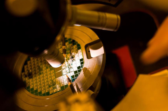
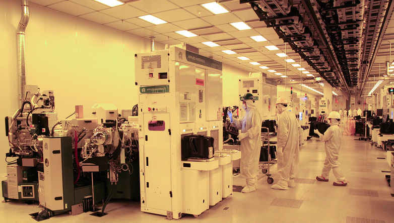
As of now, GlobalFoundries has already started to produce test wafers with circuits (IP) from a number of its customers using the 7 nm process in its Fab 8 in Malta, New York. While the company decision to skip 10nm means that it will not be able to use 10nm as a stepping-stone to 7 nm technology, it says that it has gained a lot of experience with FinFETs from the 14LPE and the 14LPP processes. The contract maker of semiconductors expects to finalize specs of its 7 nm technology in the second half of 2017, which implies on start of mass production of commercial chips in the second half of 2018. GlobalFoundries naturally does not reveal timeframes for its 7nm with EUV, but it is safe to say that EUV will be used in 2019 at the earliest.
While GlobalFoundries’ expectations for performance, power, area (PPA) improvements look solid, it should be noted that right now the contract manufacturer is among what’s become multiple companies to have confirmed their intentions to pursue a DUV-only 7 nm process technology. DUV in this respect is the tried and true approach, however in order to create 7 nm features it will require using triple/quadruple patterning, which greatly increases design and manufacturing costs as well as cycle times over previous-gen nodes. So while there is a lot of interest in using EUV if it works, many of the major fabs are starting at the same place as GlobalFoundries and at least internally preparing for DUV-only, while hoping EUV will be ready when they want it.
Case in point, Samsung currently hopes to use EUV lithography for critical layers with their 7 nm nodes to avoid triple/quadruple patterning, but are being very careful in how they’re wording their plans, saying that they are “reviewing possibilities” of EUV insertion at 7 nm. So it is not cast in stone that Samsung will not proceed with a DUV-only 7 nm if it has to. Meanwhile Intel also once considered to start using EUV for 7 nm. Finally, TSMC does not seem to be afraid of multi-patterning and intends to produce semiconductors using DUV-only 7 nm manufacturing tech in 2H 2018.
It remains to be seen how GlobalFoundries’ and TSMC’s 7 nm processes play out, but keep in mind that the former claims that its 7 nm platform is designed to be “EUV-compatible at key levels”. This means that the company will start using ASML’s TWINSCAN NXE step-and-scan systems for critical layers once they are ready (i.e., their light sources will be powerful enough for mass production and the tools will have more than 80% availability). Since GF’s 7 nm with EUV process technology will be used to produce a generation of ICs (integrated circuits) that will follow the initial 7 nm chips, GlobalFoundries makes no secret that the 7 nm with DUV and the 7 nm with EUV are essentially two different process generations (keep in mind that specs of either have not been finalized). Moreover, if EUV is ready for prime time in 2019, GF’s 7 nm DUV will be a short-lived node. In fact, GlobalFoundries is already using TWINSCAN NXEs and EUV to speed up prototyping of certain circuits for its clients.
GlobaFoundries Skips 10 nm For Two Reasons
Having announced its 7 nm manufacturing technology, GlobalFoundries confirmed rumors that it decided to skip the 10 nm fabrication process. It looks like there are at least two reasons for this decision and both lie in the PPASC (power, performance, area, schedule and costs) equation. On the one hand, the company figured out that the PPA advantages of its 10 nm technology over its 14LPP process would not be significant. On the other hand, its schedule and costs would further hinder its competitiveness. Now, let’s talk about this in a bit more detailed way.
Since manufacturing technologies are getting more complex, it is not easy to ensure that every new node offers substantial power, performance and area improvements (PPA) over the previous one. As a result, some process technologies are only used by fabless designers of semiconductors for a couple of years, whereas others are used by dozens of companies for many years. GlobalFoundries believes that 10 nm process would not provide tangible performance, power and area advantages over 14LPP process technology (which is based on 20 nm back-end-of-line interconnect flow) and would become a short-lived transitional node, hence their reason to skip it. We have seen a few such nodes in the recent years: as a limited number of firms used 45 nm, 32 and 20 nm process technologies, albeit all for different reasons.
If we take a look at the advertised PPA improvements for the most recent leading-edge process technologies from GF, Samsung and TSMC, it will be clear that transition to 10 nm node will bring improvements to TSMC’s abilities, but not by a large enough degree to satisfy all of its customers (we observed something similar with the CLN20SOC several years ago). Moreover, Samsung’s numbers are somewhat less impressive (keep in mind that GF’s 14LPP was licensed from Samsung), confirming GlobalFoundries expectations.
Advertised PPA Improvements of Leading Edge Process Technologies
Data announced by companies during conference calls, press briefings and in press releases |
| |
GlobalFoundries |
Samsung |
TSMC |
7nm DUV
vs 14LPP |
14LPP
vs 28LPP |
10LPE
vs 14LPP |
10LPP
vs 10LPE |
20SOC
vs
28 nm |
16FF+
vs
28HPM |
16FF+
vs
20SOC |
10FF
vs
16FF+ |
7FF
vs
10FF |
| Power |
>60% |
60% |
30% |
none |
25% |
70% |
60% |
40% |
<40% |
| Performance |
>30% |
40% |
>10% |
>10% |
30% |
65% |
40% |
20% |
– |
| Area Reduction |
>50% |
50% |
32% |
none |
<50% |
~50% |
none |
>50% |
>37% |
To a degree, GlobalFoundries seems to be at least partially right in its thinking of 10 nm as of a transitional node. Only three customers have taped out their 10 nm chips at TSMC so far, less than six months before TSMC intends to get its first 10 nm revenue (in Q1 2017). By contrast, tens of companies taped out their 16 nm (CLN16FF) products long before the start of high-volume production in the second half of 2015. What is more important is that according to TSMC, its 10 nm fabrication process will be mostly used by mobile SoC developers (read: Apple, Qualcomm, MediaTek), which desperately need to squeeze more transistors into new chips every year, improve performance and reduce power consumption by a bit too. Such customers are less concerned about manufacturing costs and aggressive improvements, they simply need new technologies to make certain progress due to market demands.
Meanwhile, TSMC’s 7 nm manufacturing technology will be used by multiple customers of the company, including those from high-performance computing space, the company said recently (it does not mean, though, that nobody from HPC space is going to use 10 nm). TSMC plans to start volume production of 7 nm chips in the first half of 2018, so, it is a little bit ahead of GlobalFoundries with this node. However, its first EUV-based process technology (5 nm) is scheduled for 2020, so, the company might be a little behind its rival when it comes to next-gen lithography.
Samsung demonstrated the first wafers processed using its 10LPE (10 nm, low-power early) technology in May, 2015, and disclosed plans to start volume production of chips using its 10 nm tech in late 2016. In addition, the company is planning to quickly roll-out an improved version of the tech called 10LPP, the company said earlier this year. Since Samsung needs to produce leading-edge SoC for its smartphones, it is not surprising that it is also deploying 10 nm fabrication processes: even in case it does not have a lot of foundry customers for them, it is going to need them itself to stay competitive against Apple (and potentially land Apple as a foundry client). Moreover, if Samsung requires EUV for its 7 nm process technology, it will have to use 10 nm before ASML is ready with its commercial EUV step-and-scan systems. In fact, this is why Samsung does not reveal whether it expects to start making chips using 7 nm process in 2019 or later.
Meanwhile, there is another reason why GlobalFoundries decided to skip the 10 nm fabrication technology (in addition to insignificant performance and area advantages over the 14LPP). Back in 2014, the company acquired assets of IBM Microelectronics along with a team of developers. Naturally, the integration of IBM staff took time, so instead of creating a 10 nm manufacturing process (which would be late anyway), the company decided to focus on its 7 nm technology platform. The latter will be the first process developed by the team consisting of GF and IBM developers.
Finally, keep in mind that while makers of semiconductors use terms like 7 nm or 10 nm to name their fabrication technologies, such numbers nowadays do not necessary reflect transistor density and other factors. Not all 10 nm manufacturing technologies are created equal. For example, Intel argues that transistor density of its 10 nm process is going to be comparable to transistor densities of competing 7 nm technologies. Nonetheless, a new node is still a new node with its own advantages compared to its direct, in-house predecessor.
Smooth Transition to EUV
Nowadays both semiconductor makers and manufacturers of production equipment agree that EUV will be required to make chips using smaller fabrication technologies, and the question is whether ASML will be ready with viable tools for 7 nm or for 5 nm nodes. As a result, everyone has to make decisions about when to start using EUV scanners for critical layers.
Leading-Edge Industry Lithography Roadmap, Mass Production
Data announced by companies during conference calls, press briefings and in press releases |
| |
2016 |
2017 |
2018 |
2019 |
2020 |
| 1H |
2H |
1H |
2H |
| GlobalFoundries |
14LPP |
7 nm DUV |
7nm with EUV
exact timing not announced |
| Intel |
14 nm
14 nm+ |
10 nm |
no data |
| Samsung |
14LPP
14LPC |
10LPE |
10LPP |
7LPP (7nm with EUV)
exact timing not announced |
| SMIC |
28 nm |
14 nm in development |
| TSMC |
CLN16FF+ CLN16FFC |
CLN10FF |
CLN7FF |
unknown |
5 nm EUV |
| UMC |
28 nm |
14 nm |
no data |
ASML and Cymer are making a steady progress with their EUV tools and manufacturers of semiconductors are learning how to use those tools. So far, only TSMC has publicly announced plans to use EUV for commercial 5 nm chips in 2020. Samsung has publicly mulled over using EUV tools for its 7 nm semiconductors, but it does not specify when. GlobalFoundries said that it could use EUV for its 7 nm manufacturing technology, but also did not specify exact timing. Intel is still weighing its options, hence, it is still possible that the company will start to use EUV for its 7 nm fabrication process. Meanwhile, SMIC and UMC have not specified their plans concerning next-gen lithography. In fact, both companies yet have to catch up with their rivals when it comes to FinFET first.
By developing a 7 nm process technology “compatible with EUV at key levels”, which essentially means two generations of the fabrication process, GlobalFoundries plays it safe:
- Firstly, it will have an all new process technology ready for production in 2H 2018. It is several months later than TSMC, but is still ahead of Intel and such manufacturing tech advantage could be good for AMD as well as other customers of GlobalFoundries (but bear in mind increased costs and cycle times).
- Secondly, once EUV tools are ready for prime time, GlobalFoundries will have a proven and polished-off process technology ready for EUV insertion (keep in mind that 193 nm ArF tools will be used for the majority of layers for a long time).
- Thirdly, even if ASML’s tools are not ready by 2H 2019 (something that its clients will learn well ahead of that timeframe), GlobalFoundries will have a competitive node and time to develop its next process with, or without EUV.
Of course, in certain circumstances GlobalFoundries may end up competing against TSMC’s 5 nm EUV technology with its 7 nm manufacturing process in 2020, but this is something the company is going to try to avoid.
GlobalFoundries to Offer EUV and FD-SOI
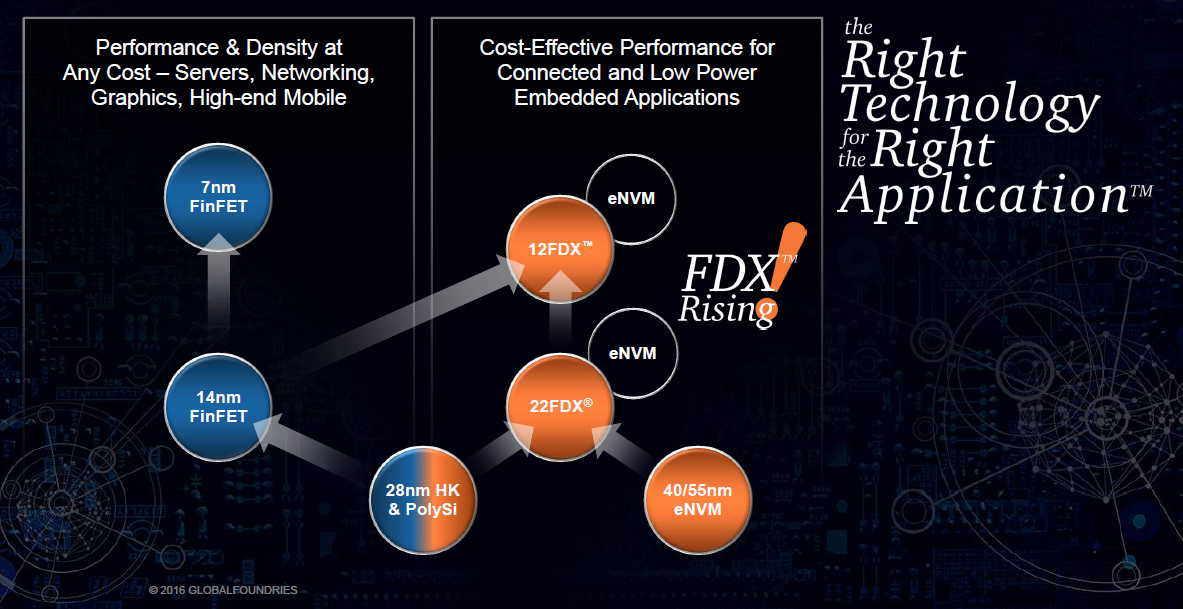
GlobalFoundries does not put all eggs in one basket. While companies like TSMC and Samsung develop low-cost/low-power versions of their FinFET manufacturing technologies in a bid to attract smaller players, GF also plans to keep developing new planar fabrication processes featuring FD-SOI. Therefore, for cost effective, low power and radio applications, the company will keep using its 22FDX (it uses back-end-of-line interconnect flow of STMicroelectronics’ 28nm FD-SOI as well as front-end of line of STM’s 14nm FD-SOI process technology) and eventually 12FDX technologies (also announced this month).

Since it is considerably cheaper to design chips featuring planar transistors, these technologies are going to be used by various smaller fabless semiconductor developers. In general, GlobalFoundries positions its 22FDX as an alternative for 14/16 nm FinFET technologies, whereas the 12FDX is going to compete against 10 nm and, possibly, sub-10 nm processes in 2019 and beyond. Samsung, another FD-SOI backer, plans to add eNVM (embedded non-volatile memory) to its 28FDS platform in 2018, but so far it has not announced any plans for a new FD-SOI technology platform.
It remains to be seen is how successful the FD-SOI offerings from GlobalFoundries will be, given the competition. Nonetheless, GlobalFoundries and Samsung are the only contract makers of semiconductors, which have announced plans to offer both leading-edge FinFET as well as planar FD-SOI manufacturing processes in 2020 and beyond. Moreover, GlobalFoundries is the only company, who disclosed plans for a sub-20 nm FD-SOI fabrication technology.