
ARM moves at an aggressive pace, pushing out new processor IP on a yearly cadence. It needs to move fast partly because it has so many partners across so many industries to keep happy and partly because it needs to keep up with the technology its IP comes into contact with, everything from new process nodes to higher quality displays to artificial intelligence. To keep pace, ARM keeps multiple design teams in several different locations all working in parallel.
At its annual TechDay event last year, held at one such facility in Austin, Texas, ARM introduced the Mali-G71 GPU—the first to use its new Bifrost GPU architecture—and the Cortex-A73 CPU—a new big core to replace the A72 in mobile. Notably absent, however, was a new little core.
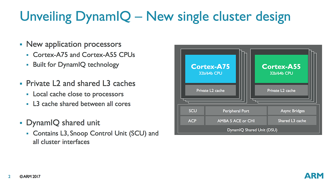
Another year, another TechDay, and another ARM facility (this time in Cambridge, UK)—can only mean new ARM IP. Over the span of several days, we got an in-depth look at its latest technologies, including DynamIQ, the Mali-G72 GPU, the Cortex-A75, and (yes, finally) the successor to the A53: Cortex-A55.
The A53 was announced alongside the A57 and has been in use for several years, both on its own or as the little core in a big.LITTLE configuration. It’s been hugely successful, with more than 40 licensees and 1.7 billion units shipped in just 3 years. But during this time ARM introduced new big cores on a yearly cadence, moving from A57 to A72 to A73. The A53 remained unchanged, however, even as the performance gap between the big and little cores continued to grow.
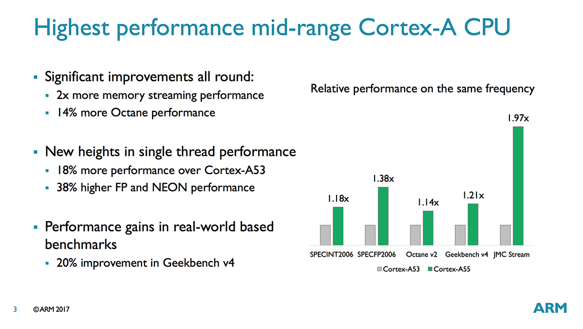
Predictably then, the focus for A55 was on improving performance. The A53’s dual-issue, in-order core, which serves as the starting point for A55, already delivers good throughput, so ARM focused on improving the memory system. A new data prefetcher, an integrated L2 cache that reduces latency by 50%, and an extra level of L3 cache (among other changes) give the A55 significantly better memory performance—quantified by a nearly 2x improvement in the LMBench memory copy test. The numbers provided by ARM also show an 18% performance gain in SPECint 2006 and an even bigger 38% gain in SPECfp 2006 relative to the A53. These numbers, as well as the others shown in the chart, comparing the A55 and A53 are at the same frequency, same L1/L2 cache sizes, same compiler, etc. and are meant to be a fair comparison. The actual gains should actually be a little higher, because partner SoCs will benefit from adding the L3 cache, which these numbers do not include.
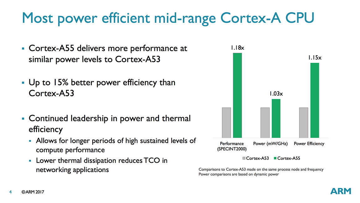
The additional performance does not come for free, however. Power consumption is up 3% relative to the A53 (iso-process, iso-frequency), but power efficiency still improves by 15% when running SPECint 2000 because of its higher performance.
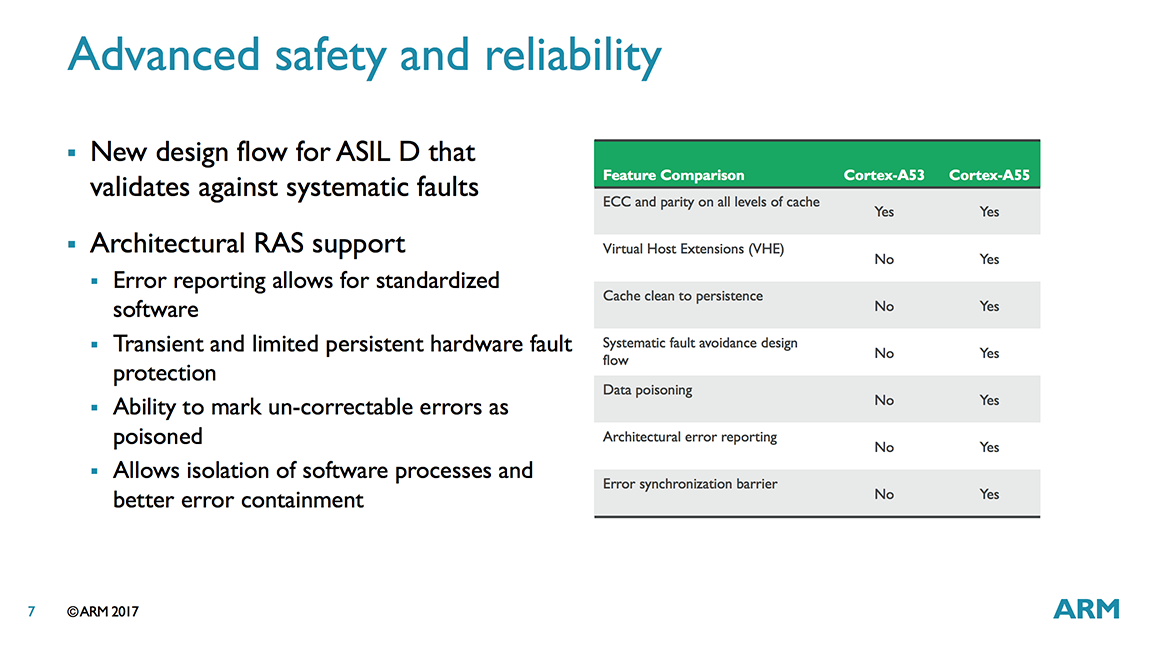
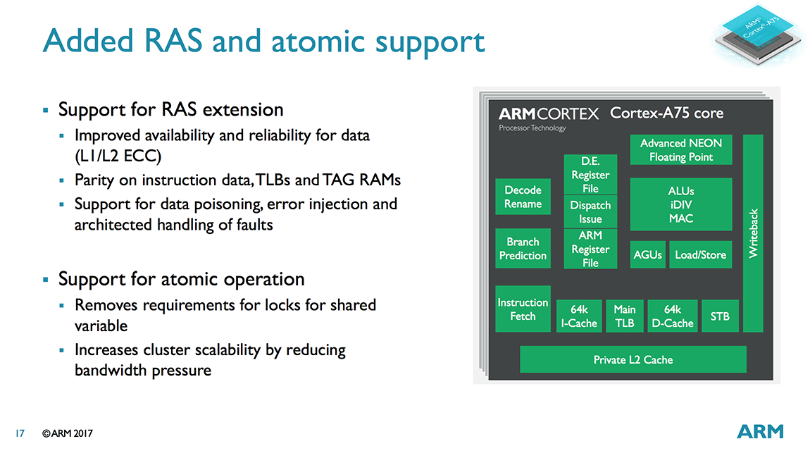
The A55 includes several new features too that will help it expand into new markets. Virtual Host Extensions (VHE) are very important for the automotive market and the advanced safety and reliability features, including architectural RAS support and ECC/parity for all levels of cache are critical for many applications, including automotive and industrial. There’s new features for infrastructure applications too, including a new Int8 dot product instruction (useful for accelerating neural networks). Because A55 is compatible with DynamIQ, it also gets cache stashing and access to a 256-bit AMBA 5 CHI port.
When ARM announced the A73 last year, it talked a lot about improving sustained performance and working within a tight thermal envelope. In other words, the A73 was all about improving power efficiency. The A75 goes in a different direction: Taking advantage of the A73’s thermal headroom, ARM focused on improving performance while maintaining the same efficiency as the A73.
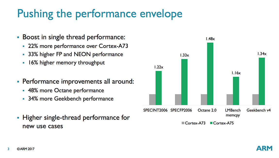
Our previous performance testing revealed mixed results when comparing the A73 to the A72—not too surprising given the significant differences in microarchitecture—with the A73 generally outpacing the A72 by a small margin for integer tasks but falling behind the older CPU in floating point workloads. Things look better for the A75, at least based on ARM’s numbers, which show noticeable gains over the A73 in both integer and floating-point workloads as well as memory streaming.
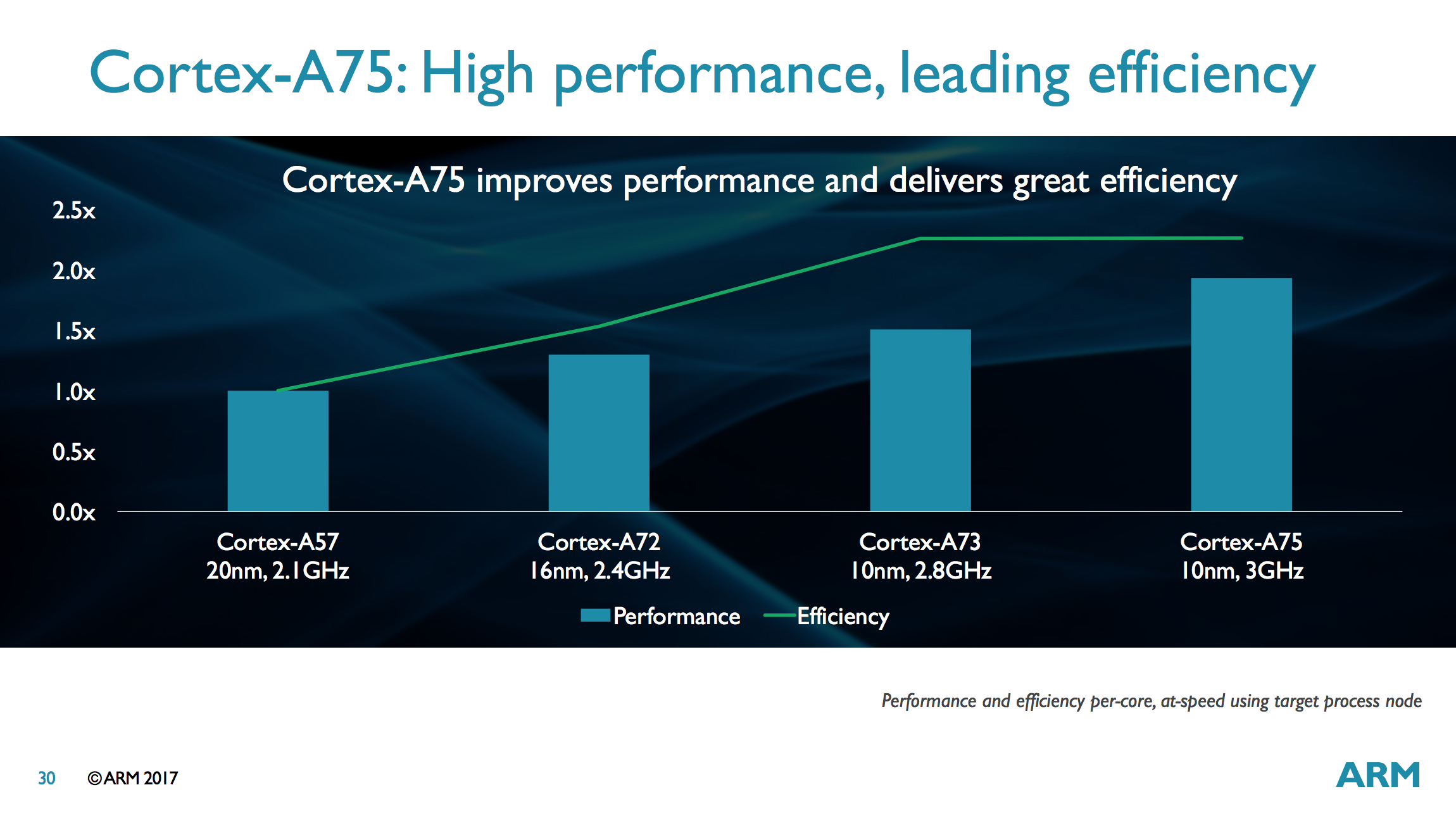
The graph above shows that the A75 operating at 3GHz on a 10nm node achieves better performance and the same efficiency as an A73 operating at 2.8GHz on a 10nm node, which means the A75 consumes more power. How much more is difficult to tell based on this one simple graph. We know that the A73 is thermally limited when using 4 cores (albeit less so than the A72), so the A75 definitely will be as well. This is not a common scenario, however. Most mobile workloads only fire up 1-2 cores at a time and usually only in short bursts. ARM obviously felt comfortable enough using the A73’s extra thermal headroom to boost performance without negatively impacting sustained performance.
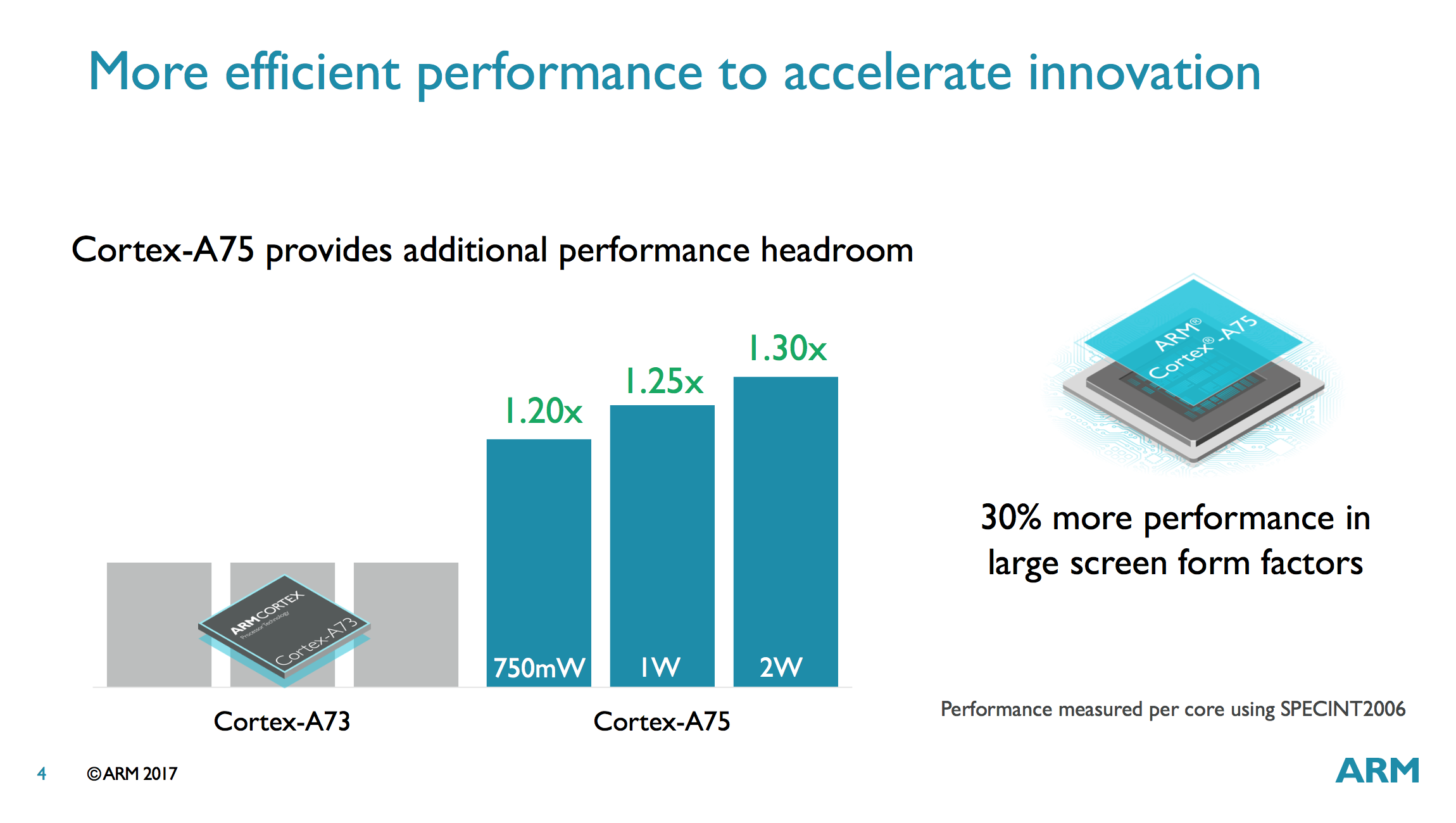
ARM wants to push the A75 into larger form-factor devices with power budgets beyond mobile’s 750mW/core too by pushing frequency higher. Something like a Chromebook or a 2-in-1 ultraportable come to mind. At 1W/core the A75 delivers 25% higher performance than the A73 and at 2W/core the A75’s advantage bumps up to 30% when running SPECint 2006. If anything, these numbers highlight why it’s not a good idea to push performance with frequency alone, as dynamic power scales exponentially.
ARM targeted the A73 specifically at mobile by focusing on power efficiency and removing some features useful for other applications to simplify the design, including no ECC on the L1 cache and no option for a 256-bit AMBA 5 CHI port. With A75, there’s now a clear upgrade path from A72. For the server and infrastructure markets, A75 supports ECC/parity for all levels of cache and AMBA 5 CHI for connecting to larger CCI, CCN, or CMN fabrics, and for automotive and other safety critical applications there’s architectural RAS support, protection against data poisoning, and improved error management.
On the next few pages, we’ll dive deeper into the technical details and features of ARM’s new IP, including DynamIQ (the next iteration of big.LITTLE), Cortex-A75, and Cortex-A55.
Before we discuss the new CPUs, we need to discuss DynamIQ. Introduced 5 years ago, ARM’s original big.LITTLE (bL) technology, which allows multiple clusters of up to 4 CPUs to be chained together, has been massively successful in the marketplace, allowing various combinations of its Cortex-A family of CPUs to power mobile devices ranging from the budget-friendly with no frills to the budget-busting flagships stuffed with technology. The combination of Cortex-A and bL extends beyond smartphones and tablets too, with applications ranging from servers to automotive.
Over the years, ARM’s IP and the needs of its customers have evolved, necessitating a new version of bL: DynamIQ. ARM started working on DynamIQ in 2013 by asking a single question: “How do you make big.LITTLE better?” Looking forward, ARM could see DynamIQ needed to be more flexible, more scalable, and offer better performance. Considering how much work went into this project, DynamIQ will be around for at least the next few years, so hopefully it delivers on those goals.
Like bL, DynamIQ provides a way to group CPUs into clusters and connect them to other processors and hardware within the system; however, there’s several significant changes, starting with the ability to place big and little Cortex-A CPUs in the same cluster. With bL, different CPUs had to reside within separate clusters. What appears to be a simple reshuffling of cores actually impacts CPU performance and configuration flexibility.
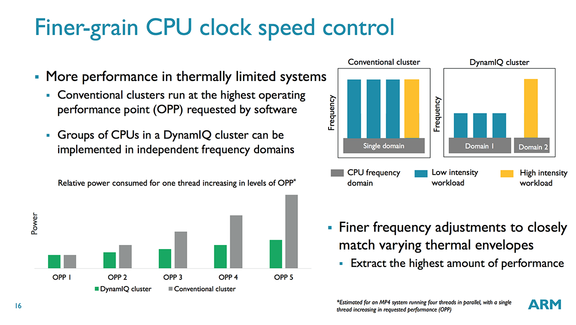
Another big change is the ability to place up to 8 CPUs inside a single cluster (up from 4 for bL), with the total number of CPUs scaling up to 256 with 32 clusters, which can scale even further to 1000s of CPUs with multi-chip support provided via a CCIX interface. Within a cluster CPUs are divided into voltage/frequency domains, and within a domain each core is inside its own power domain. This allows each CPU to be individually powered down, although all CPUs in the same domain must operate at the same frequency, which is no different from bL; however, with DynamIQ each cluster can support up to 8 voltage/frequency domains, providing greater flexibility than bL’s single voltage/frequency domain per cluster. So, what does this mean? It means that, in theory, an SoC vendor could place each CPU into its own voltage domain so that voltage/frequency could be set independently for each of the 8 CPUs in the cluster. Each voltage/frequency domain requires its own voltage regulator, which adds cost and complexity, so we’ll most likely continue to see 2-4 CPUs per domain.
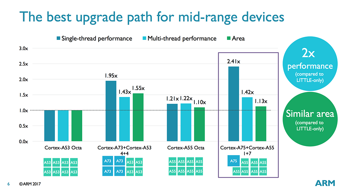
ARM still sees 8-core configurations being used in mobile devices over the next few years. With bL, this would likely be a 4+4 pairing using 4 big cores and 4 little cores or 8 little cores spread across 2 clusters. With DynamIQ, all 8 cores can fit inside a single cluster and can be split into any combination (1+7, 2+6, 3+5, 4+4) of A75 and A55 cores. ARM sees the 1+7 configuration, where one A55 core is replaced by a big A75 core, as particularly appealing for the mid-range market, because it offers up to 2.41x better single-thread performance and 1.42x better multi-thread performance for only a 1.13x increase in die area compared to an octa-core A53 configuration (iso-process, iso-frequency).
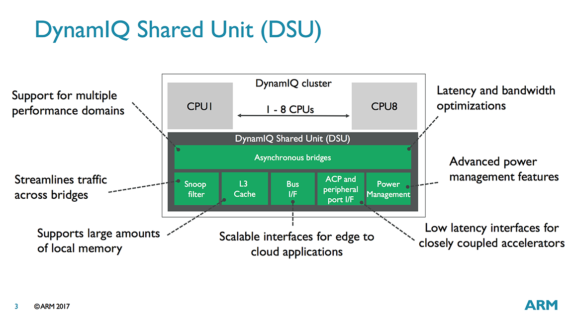
The main puzzle piece that enables this flexibility is the DynamIQ Shared Unit (DSU), a separate block that sits inside each DynamIQ cluster and functions as a central hub for the CPUs within the cluster and the bridge to the rest of the system. Each voltage/frequency domain in the cluster can be configured to run synchronously or asynchronously with the DSU. Using asynchronous bridges (one per domain) allows different CPUs (A75/A55) to operate at different frequencies (using synchronous bridges would force all CPUs to operate at the same frequency).
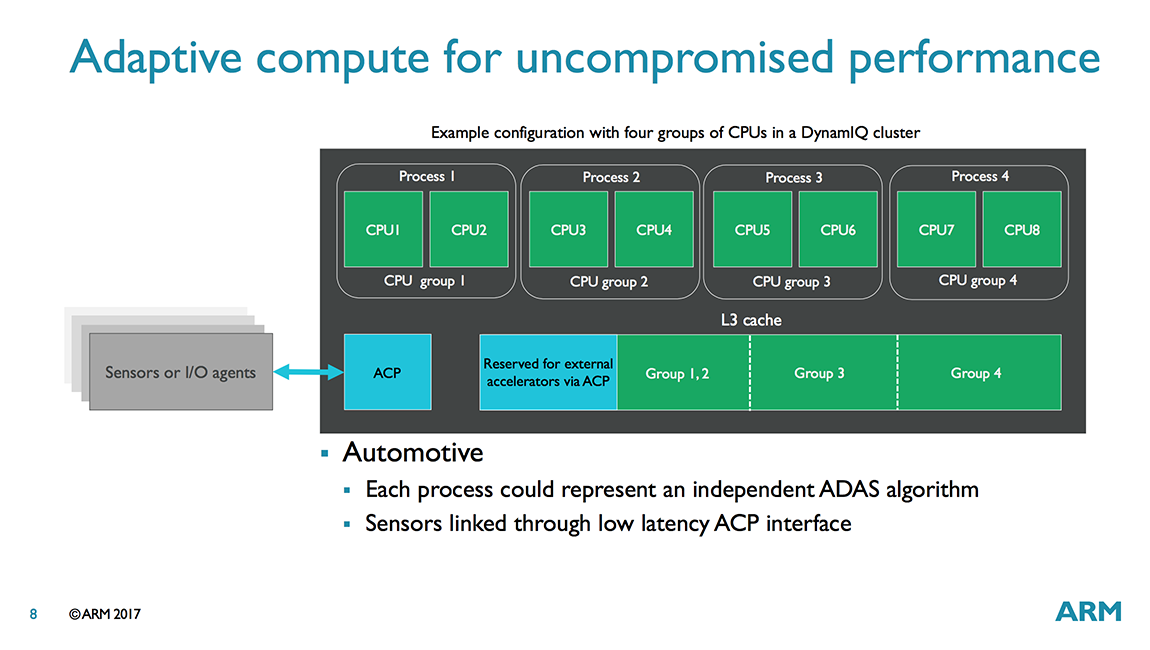
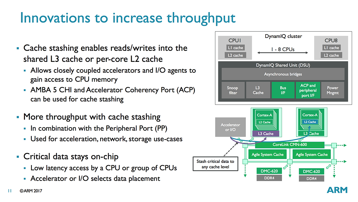
The DSU communicates with a CCI, CCN, or CMN cache-coherent interconnect through 1 to 2 128-bit AMBA 5 ACE ports or a single 256-bit AMBA 5 CHI port. There’s also an Accelerated Coherency Port (ACP) for attaching specialized accelerators that require cache coherency with the CPUs. It’s also used for enabling DynamIQ’s cache stashing feature, which we’ll discuss in a minute. Finally, there’s a separate peripheral port that’s used to program the accelerators attached to the ACP interface (basically a shortcut for programming transactions so they do not need to be routed through the system interconnect).
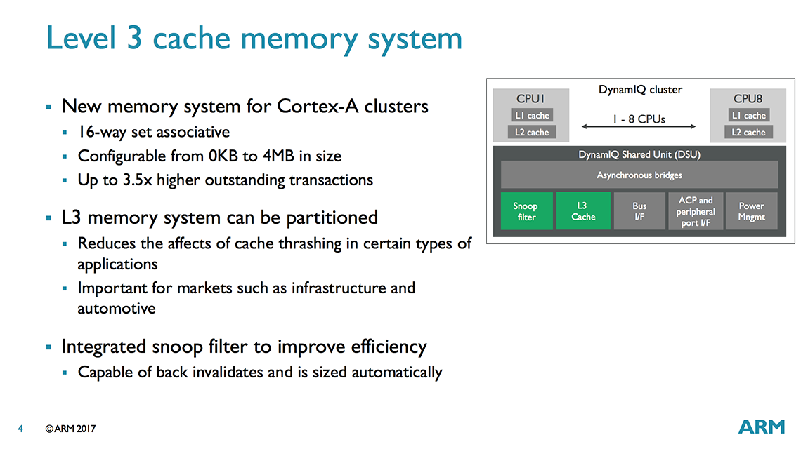
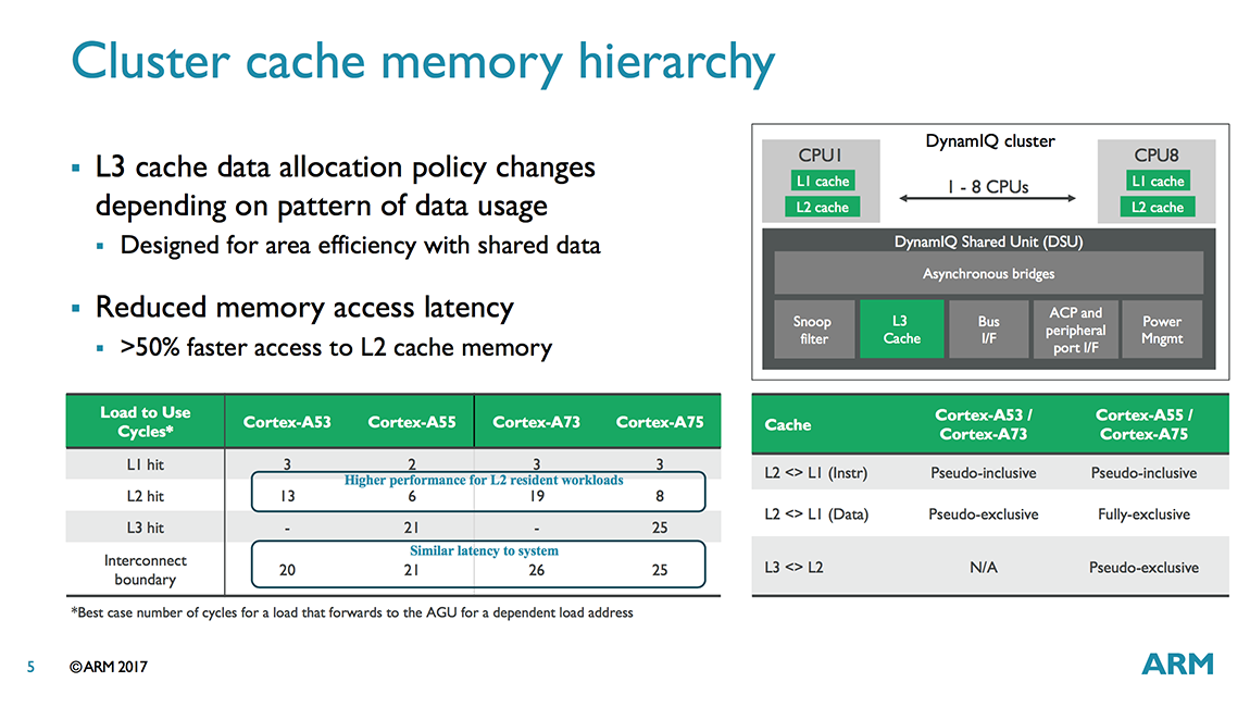
So far we’ve discussed DynamIQ’s flexibility and scalability features, but it also improves CPU performance through a new cache topology. With bL, CPUs inside a cluster had access to a shared L2 cache; however, DynamIQ compatible CPUs (currently limited to A75/A55) have private L2 caches that operate at the CPU core’s frequency. Moving the L2 closer to the core improves L2 cache latency by 50% or more. DynamIQ also adds another level of cache: The optional shared L3 cache lives inside the DSU and is 16-way set associative. Cache sizes are 1MB, 2MB, or 4MB, but may be omitted for certain applications like networking. The L3 cache is technically pseudo-exclusive, but ARM says it’s really closer to being fully-exclusive, with nearly all of the L3’s contents not appearing in the L2 and L1 caches. If the new L3 cache was inclusive, meaning that it contained a copy of a CPU’s L2, then its performance benefit would be largely mitigated and a lot of area and power would be wasted.
The L3 cache can be partitioned, which can be useful for networking or embedded systems that run a fixed workload or applications that require more deterministic data management. It can be partitioned into a maximum of 4 groups, and the split can be unbalanced, so 1 CPU could get 3MB while the other 7 CPUs would share the remaining 1MB in an 8-core 4MB L3 configuration. Each group can be assigned to specific CPU(s) or external accelerators attached to the DSU via the ACP or other interface. Any processors not specifically assigned to a cache group share the remaining L3 cache. The partitions are dynamic and can be created/adjusted during runtime by the OS or hypervisor.
One of the features supported by DynamIQ is error reporting, which allows the system to report detected errors, both correctable and uncorrectable, to software. The L3 supports ECC/parity (actually all levels of cache and snoop filters do, with SECDED on caches that can hold dirty data and SED parity on caches that only hold clean data) in order to be ASIL-D compliant. The L3 also has persistent error correction and can support recovery from a single hard error (data poisoning is supported at a 64-bit granularity).
Another new feature is cache stashing, which allows a GPU or other specialized accelerators and I/O agents to read/write data into the shared L3 cache or directly into a specific CPU’s L2 cache via the ACP or AMBA 5 CHI port. A specific example is a networking appliance that uses a TCP/IP offload engine to accelerate packet processing. Instead of writing its data to system memory for the CPU to fetch or relying on some other cache coherency mechanism, the accelerator could use cache stashing to write its data directly into the CPU’s L2, increasing performance and reducing power consumption.
In order to use cache stashing, the software drivers running in kernel space need to be aware of the processor and cache topology, which will require custom code to enable hardware outside the cluster to access the shared L3 or an individual CPU’s L2. While a limitation for consumer electronics where time to market is key, it’s not as serious of an issue for commercial applications.
While cache stashing could be a useful feature for sharing data with processors sitting outside the cluster, DynamIQ also makes it easier to share data among CPUs within a cluster. This is one of the reasons why ARM wanted to bring big and little CPUs into the same cluster. Moving cache lines within a DynamIQ cluster is faster than moving them between clusters like with bL, reducing latency when migrating threads between big and little cores.

DynamIQ also includes improved power management. Having the DSU perform all cache and coherency management in hardware instead of software saves several steps when changing CPU power states, allowing the CPU cores to power up or down much faster than before with bL. The DSU can also power down portions of the L3 cache to reduce leakage power by autonomously monitoring cache usage and switching between full on, half off, and full off states.
The DSU includes a Snoop Control Unit (SCU) with an integrated snoop filter for handling the new cache topology. Together with L3 cache and other control logic, the DSU is about the same area as an A55 core in its max configuration or half the area of an A55 in its min configuration. These are just rough estimates because most of the DSU area is used by the L3 cache and the size of the DSU logic scales with the number of CPU cores.
Some of ARM’s partners may be slow to migrate from bL to DynamIQ, choosing to stick with a technology and CPU cores they are familiar with instead of investing the extra time and money required to develop new solutions. But for performance (and marketing) sensitive markets that need access to ARM’s latest CPU cores, such as mobile, the switch to DynamIQ should happen quickly, with the first DynamIQ SoCs likely to appear by the end of 2017 or early 2018.
The Cortex-A75 is the newest member of ARM’s Sophia family of CPUs, which also includes the A73, A17, and A12. It’s no surprise then that the A75 and A73 have much in common just like the A72 and A57 before them (both of which belong to the Austin CPU family); however, ARM’s focus has shifted from improving power efficiency and thermal headroom for A73 to improving performance and adding new features for A75. ARM addressed its performance goals through significant changes to the pipeline and support for DynamIQ, while the new features are a byproduct of moving from the ARMv8.0 architecture to ARMv8.2. For this article, I’m primarily going to focus on what’s new for A75, so I recommend reading our introduction to the A73 to get a more complete understanding of the A75 microarchitecture.
The A75 uses a relatively short 11-13+ stage (depending on instruction type) out-of-order pipeline similar to the A73. Instruction fetch is still 4 stages and the decoder is still able to decode most instructions in a single cycle, with µops destined for the NEON/FP (floating-point) pipelines requiring an additional decode stage; however, moving to 3-wide decode makes the A75 is a wider machine than A73, a big change that will be discussed in greater detail below.
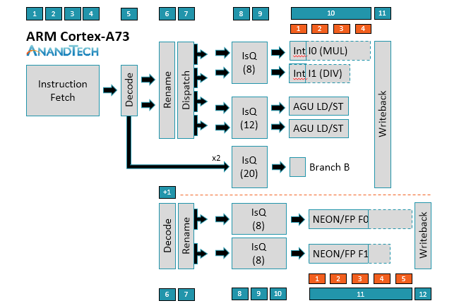
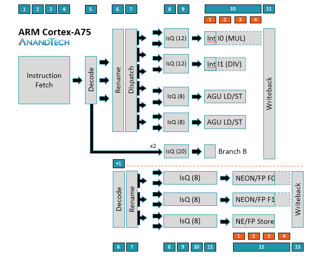
The ability to decode up to 3 instructions/cycle means A75 can now dispatch up to 6 µops/cycle instead of 4 µops/cycle for A73. On the integer side, the A75 can feed up to 2 µops into each issue queue. Instead of shared issue queues for the 2 ALUs and 2 AGUs, each pipe in A75 gets its own issue queue with more entries. This allows the A75 to be more speculative, improving its ability to execute instructions out of order and continue operation during an L1 D-cache miss that hits in L2, for example. The peak issue rate increases to 8 µops/cycle, 1 for each pipe.
As the diagrams for A73/A75 show, simple branch µops can bypass Rename and Dispatch, effectively removing 2 stages of latency; however, more complex branch instructions that require access to registers can spawn additional branch, AGU, and ALU µops that require passing through Rename/Dispatch, with some additional complexity hidden within the Rename stage.
Moving to the NEON/FP side, you’ll notice that there’s no Dispatch stage for A73/A75. Obviously, µops are still being pushed into the issue queues, and there’s still load balancing between queues, but it’s handled differently and one reason why the issue queues are 1-2 stages longer than those on the integer side.
There have been some changes to the NEON/FP side as well. The A75 can now “dispatch” up to 3 µops/cycle and sink up to 2 µops into each issue queue, which grow to 4 stages deep instead of 3 for A73. ARM looked at increasing the number of entries in the issue queues too, but it found this increased power more than performance, so it nixed the idea. Instead it added a dedicated NEON/FP store pipe with its own issue queue. The latency of a FP multiply-accumulate (MAC) has also been reduced to 5 cycles compared to 6 cycles on A73.
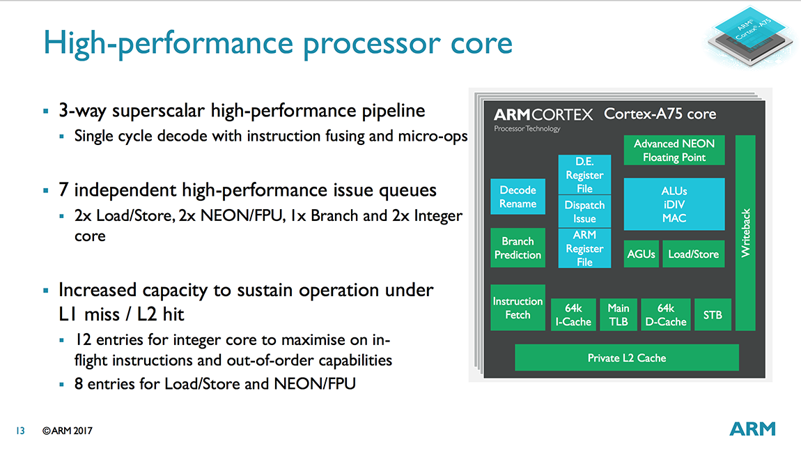
I’ll discuss the execution pipelines in greater detail as we work our way through the data path, but let’s start on the instruction side first. The A75 is still a “slot-based microarchitecture,” which was first introduced with the A73. ARM is not disclosing any additional details beyond its basic explanation from last year, namely that there are 8 “slots” that work to eliminate redundant access to resources within the instruction block, which ultimately reduces power consumption.
Both the A73 and A75 have a very simple instruction prefetcher that feeds into a fixed 64KB L1 I-cache that is 4-way set associative and uses a VIPT (Virtually Indexed, Physically Tagged) access scheme, common for L1 caches because of their sensitivity to latency.
The A73 received a completely new main branch predictor, along with a new 64-entry micro-BTAC for accelerating predictions. In addition to the main predictor, there’s also a static branch predictor, which is used as a fallback when the main predictor has insufficient history, and a return stack, which contains nested subroutine return addresses. An indirect predictor, which is only used when necessary (reducing its power penalty because indirect branches occur less frequently), uses a 2-way 256-entry BTAC (Branch Target Address Cache).
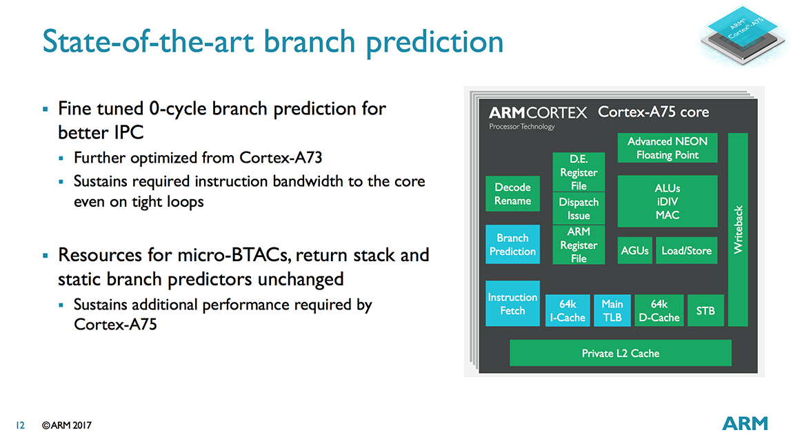
While designing the A75, ARM found that the A73’s branch predictor still performed well and that improving performance further resulted in diminishing returns, with power climbing faster than performance; therefore, the A73’s predictor was carried over to the A75. ARM did fine tune the 0-cycle micro-predictors, which sit upstream of the main predictor, improving IPC by further reducing the likelihood of pipeline bubbles in tight loops.
As I mentioned above, the A75 moves to a 3-wide instruction decode stage, up from 2-wide for the A73 and matching the 3-wide A72. ARM is always looking for ways to improve IPC (Instructions Per Cycle), and it noted that while running SPECint 2006 the A73 achieves an IPC of roughly 1.2 overall, increasing to 1.6 to 1.8 at specific sections within the test and dipping to 0.4 to 0.6 in others. Even much larger CPUs achieve an average IPC of just over 2. This does not mean you only need a 2-wide decoder, however, because there are situations that require greater throughput. For example, after a branch mispredict that requires a pipeline flush—which may occur 2-4 times for every 1000 instructions—the CPU needs to refill the issue queues as fast as possible so it can begin extracting ILP. So going wider helps throughput when you need a sudden burst of instructions. There’s a power and area penalty for going wider of course, because it causes a ripple effect through the rest of the pipeline, but it was clear to ARM that moving to 3-way superscalar was necessary to meet its IPC goals.
The A75’s Rename and Dispatch stages are similar to the A73’s. Like the A73 and other Sophia CPUs, there’s no reorder buffer or architectural register file in the A75. Instead it uses a physical register file for storing µop operands, reducing power by limiting the amount of data moving around the CPU and eliminating some instruction window bottlenecks that arise from using a reorder buffer.
The A75 does see some optimizations here, including the ability for loads to bypass writes, improving the core’s ability to execute out of order and better cope with an L2 cache miss. ARM also found that certain instructions that get cracked during the decode stage (because they need access to the register file during rename) were using too many entries in the A73’s issue queues, so the A75 now recombines these back into a single instruction after the rename stage, freeing up space in the issue queues for other µops.
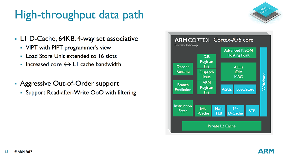
Moving over to the data path, we find an improved data prefetcher. The L1 and L2 prefetchers were already overhauled for A73, but the stride prefetcher has been retuned to better handle out of order execution for A75.
The 64KB L1 D-cache carries over nearly unchanged from A73. This is VIPT like the L1 I-cache, which reduces latency by performing the cache index lookup in parallel with the TLB translation. The A73/A75 handle aliasing issues, where several virtual addresses might reference the same physical address, in hardware, making the 4-way set associative VIPT cache look like a PIPT 8-way 32kB or 16-way 64KB cache to the programmer.
The A75 gets an integrated L2 cache that operates at core speed, reducing latency by more than 50% compared to the A73 that shares an L2 cache with the other CPUs in the same cluster. For instruction fetch, latency drops from 20-25 cycles to 11 cycles (10 cycle for a L1 miss, L2 hit), and for the lowest latency scenario (a load that forwards to the AGU because of a dependent load address) latency drops from 19 cycles to 8 cycles.
The optional L2 cache can be either 256KB or 512KB. Choosing the 512KB option only improves performance by about 2% compared to 256KB for a single core, but provides a better 4-5% uplift when using 4 A75 cores with DynamIQ. The L1 D-cache and L2 are now fully-exclusive instead of pseudo-exclusive like A73, which saves area because data is not duplicated in the L2 cache. The L1 I-cache is pseudo-inclusive.
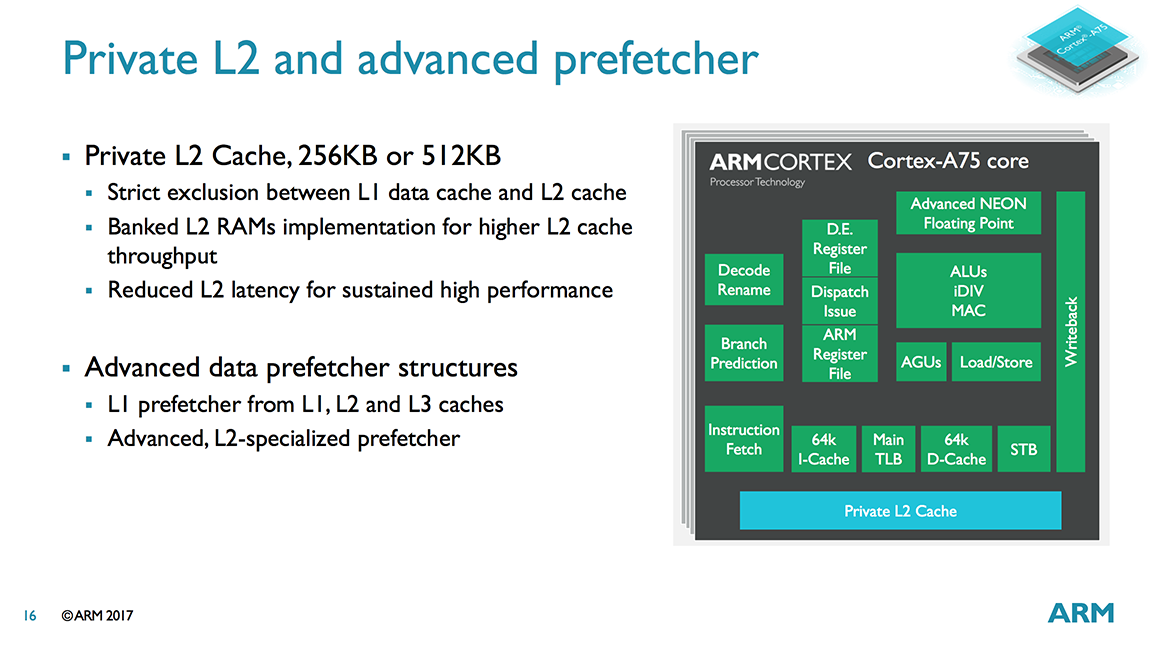
ARM improved the overall L2 hit rate by biasing the L2 cache replacement policy to have a higher affinity for instructions. The L2’s higher hit rate and lower latency improves performance but also saves power and area by allowing the A75 to continue using a very simple instruction prefetcher.
The A75’s main TLB is now non-blocking with a two outstanding fetch capability including hit under miss (the A73 main TLB is a blocking design). This change improves performance when there’s a TLB miss requiring a page table walk in main system memory. With a non-blocking TLB, it can continue to process translation requests while waiting for the page table walk to complete, which takes a comparatively long time because it requires multiple memory accesses.
Our trip through the data side of the A75’s memory system ends with the AGUs (Address Generation Units). Another carry over from the A73, the two AGUs are capable of performing both loads and stores, offering greater flexibility and a higher issue rate into the memory system. The size of the store buffer (STB), where all stores are pushed once they’ve been committed and are no longer speculative, increases to 7 128-bit slots.
Now it’s time to shift our focus to the execution pipelines. The A75’s ALU/INT pipes are the same as A73. Both ALUs can perform basic operations such as additions and shifts, but only one ALU handles integer multiplication and multiply-accumulate operations, while the other focuses on integer division. This means the A73/A75 cannot perform two integer multiplies or divides in parallel, but it can dual issue a MUL/MAC alongside a divide/add/shift. While nearly all instructions complete in 1 or 2 cycles, an integer divide takes 3 cycles and a multiply requires 4 cycles. It’s interesting that after making the move to 3-wide decode, ARM considered adding a third ALU/INT pipe; however, the performance increase was not enough to justify the increase in power.
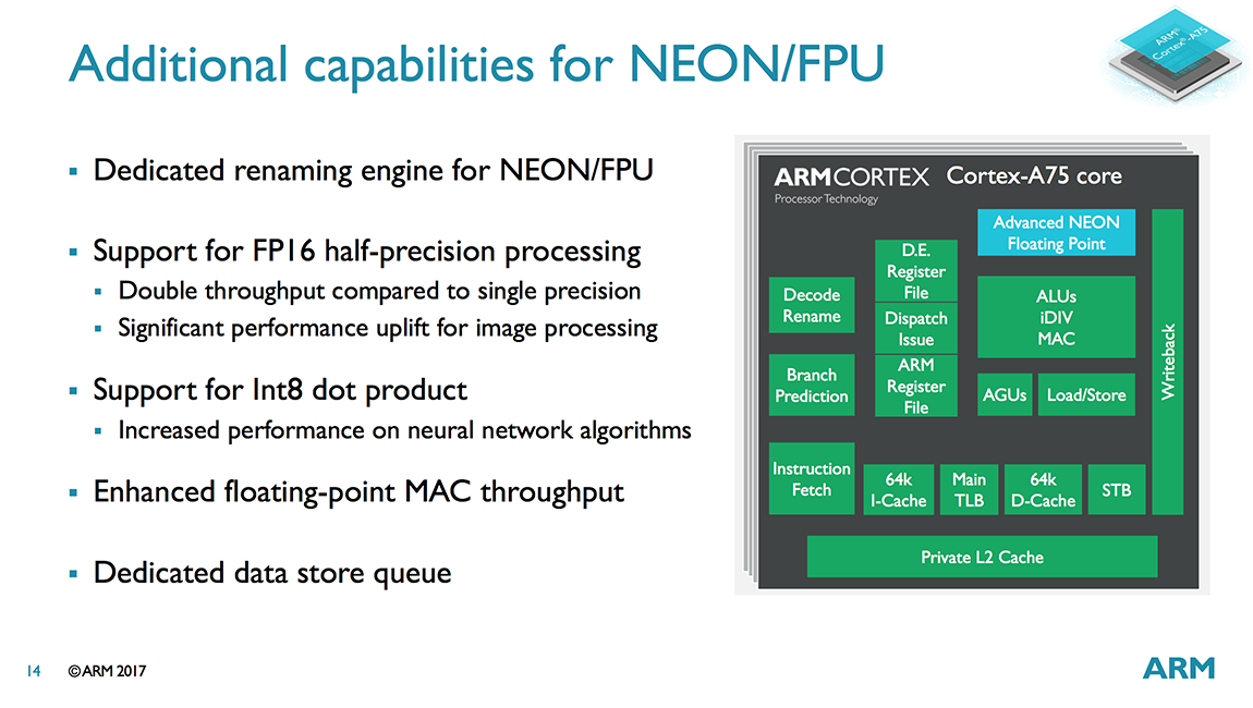
The 2 64-bit NEON/Floating Point pipes have their own dedicated Rename stage and 128-bit register file, with each SIMD NEON pipe in the A73/A75 capable of performing 8 8-bit integer, 4 16-bit integer, 2 32-bit integer or single-precision floating-point (FP), or 1 64-bit integer or double-precision FP operations per cycle, giving programmers the flexibility to choose the right balance between precision and performance.
The A75 also gains native support for half-precision FP16 operations by updating to the ARMv8.2 architecture. Using less precise data types (16-bits for FP16 versus 32- or 64-bits) reduces the amount of memory/cache required to store data and improves memory bandwidth, which can be a desirable trade-off for certain applications like machine learning and image processing. The A73 and earlier big cores could fetch FP16 values, but they need to be converted to FP32 before execution, resulting in some additional overhead.
Looking to improve performance, many neural-network algorithms are dropping down to 8-bit precision, especially after training is complete. To speed up these algorithms, the A75 (courtesy of the ARMv8.2 architecture) includes a new INT8 dot product instruction, which combines multiple instructions that required being executed back to back to back into a single instruction, significantly improving latency.
Starting with the A73 microarchitecture, ARM worked to improve IPC by moving to 3-wide decode and improving the core’s out-of-order capability, while DynamIQ support means a higher performing integrated L2 cache backed by a new L3 cache. The ARMv8.2 architecture also provides new features and new NEON instructions for accelerating neural networks and image processing.
The Cortex-A55 is the next CPU microarchitecture in ARM’s Cambridge family of low-power, small-footprint cores, which also include the A5, A7, and A53. This new little core is an evolution of the A53, so the two cores share much in common. Using the A53 as the starting point makes sense—it has proven to be a successful design—but as the big cores evolved over time, the performance gap between the big cores and the A53 grew, altering the balance in ARM’s big.LITTLE scheme. And as ARM continues its push into new markets beyond mobile, it needs new features that the A53 lacks. The A55 addresses the performance issue with improvements to the memory system and other microarchitectural changes and adds key features by moving from the ARMv8.0 architecture to ARMv8.2.
At a high level, the A55 is still a dual-issue, in-order CPU with an 8-stage pipeline. According to ARM, 8 stages is still the sweet spot, because it’s not seeing significant frequency improvements when moving from 16/14nm to 10nm to 7nm (most of the process gains are with area scaling and reduced dynamic/leakage power). With 8 stages, the A55 should reach a similar peak frequency as A53. Moving to a shorter pipeline would reduce the max frequency without a significant improvement to power or area, while a longer pipeline would increase area and power consumption for only a small frequency gain.
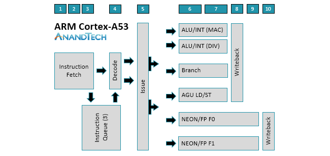
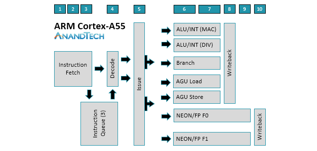
The similarities between the two cores is evident when examining the diagrams above. There’s still a 2-wide decode stage that decodes most instructions in a single cycle. Another feature that carries over from A53 is symmetric dual-issue for most instructions, meaning both issue slots can feed instructions to any pipeline. We’ll cover the execution pipelines in more detail below, but the big change here is that the A55 moves to independent load and store AGUs that can perform loads and stores in parallel instead of a single, combined AGU like the A53.
The A53’s core already provides good throughput, but not having instructions or data ready to process, perhaps because of a mispredicted branch or a cache miss, nullifies this advantage. Without the ability to execute instructions out of order while the CPU waits to fetch an instruction or data from elsewhere in the memory hierarchy, the entire core can stall (all other instructions need to wait for the current instruction to finish), so keeping an in-order core fed with instructions and data is critical. This is why ARM focused heavily on improving the A55’s memory system performance.
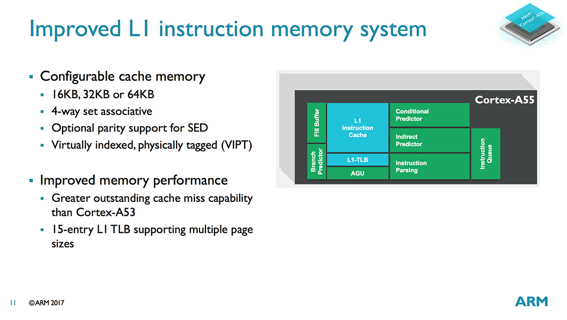
Starting on the instruction side, the L1 I-cache is now 4-way set associative versus 2-way for the A53. It’s still VIPT (Virtually Indexed, Physically Tagged), which is commonly used for L1 caches as it reduces latency, but there’s a larger 15-entry L1 TLB that supports multiple page sizes. This simple-sounding change actually required a significant amount of work to alleviate issues with timing pressure. The size of the L1 I-cache is configurable with options for 16KB, 32KB, or 64KB, which is similar to the A53 that offers a range from 8KB to 64KB.
It seems that every new CPU microarchitecture comes with a new branch predictor, and the A55 is no exception. The new conditional predictor increases prediction accuracy by using neural network based algorithms. It also adds loop termination prediction, which avoids a mispredict occurring at the end of a loop. There are also new 0-cycle micro-predictors ahead of the main conditional predictor. These are not as accurate as the main predictor, but their ability to perform predictions back to back to back provide a significant performance uplift by reducing pipeline bubbles even in tight loops. There’s also an indirect predictor that’s only used when necessary, reducing the power penalty because indirect branches do not occur as frequently. This includes a 256-entry BTAC (Branch Target Address Cache).
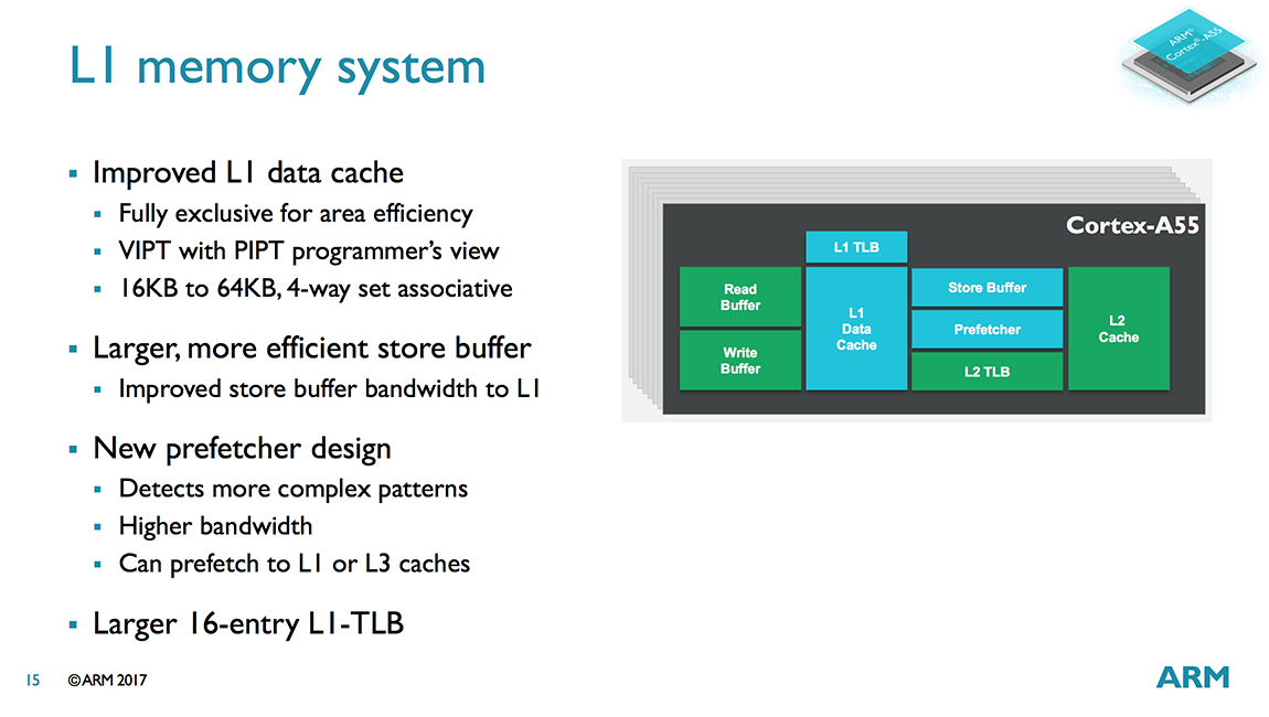
Switching over to the data path, the A55 includes an improved data prefetcher that delivers higher bandwidth. It’s capable of detecting more complex cache miss patterns and can prefetch to the L1 or L3 caches. ARM expects these improvements to make a noticeable impact on mobile device UI performance.
The L1 D-cache is still 4-way set associative like the A53, but is now fully-exclusive instead of pseudo-exclusive, which saves area because data is not duplicated in the L2 cache. The size of the L1 D-cache is also configurable with 16KB, 32KB, or 64KB options, which is also similar to the A53’s range from 8KB to 64KB.
Another big change for the L1 D-cache is moving from a PIPT (Physically Indexed, Physically Tagged) to a VIPT access scheme. This reduces cache latency because the cache index lookup happens in parallel with the TLB translation, but also creates aliasing issues where several virtual addresses might reference the same physical address. The A55 deals with aliasing in hardware, however, making the VIPT cache appear like a PIPT cache to the programmer.
Further enhancements include a larger 16-entry micro-TLB for the L1 D-cache, a significant increase over the A53’s 10-entry micro-TLB, and a larger store buffer with higher bandwidth into the L1 to better cope with workloads that generate a lot of stores. ARM also reduced the L1 pointer chasing load-to-use latency from 3 cycles in A53 to 2 cycles in A55, providing a small performance bump when working with certain types of data structures.
Being compatible with DynamIQ means the A55 gets an integrated L2 cache that operates at core speed. This reduces L2 latency by 50% (12 cycles to 6 cycles) compared to the A53 and its shared L2. The L2 cache size options include 0KB, 64KB, 128KB, and 256KB. ARM expects 128KB to be the most common for mobile applications, but there should be a reasonable number of 256KB configurations too. The smaller sizes will appeal to the networking and embedded markets that desire lower area/cost or need more deterministic memory behavior. With the L2 now part of the core, the A55’s L2 TLB grows to 1024 entries up from 512 entries for A53.
The A55’s integrated L2 uses PIPT, which is simpler to implement and uses less power than VIPT. Unlike the VIPT L1, using PIPT for the L2 does not incur a performance penalty because its naturally higher latency means there’s sufficient time to get the physical address from the TLB before performing the tag compare.
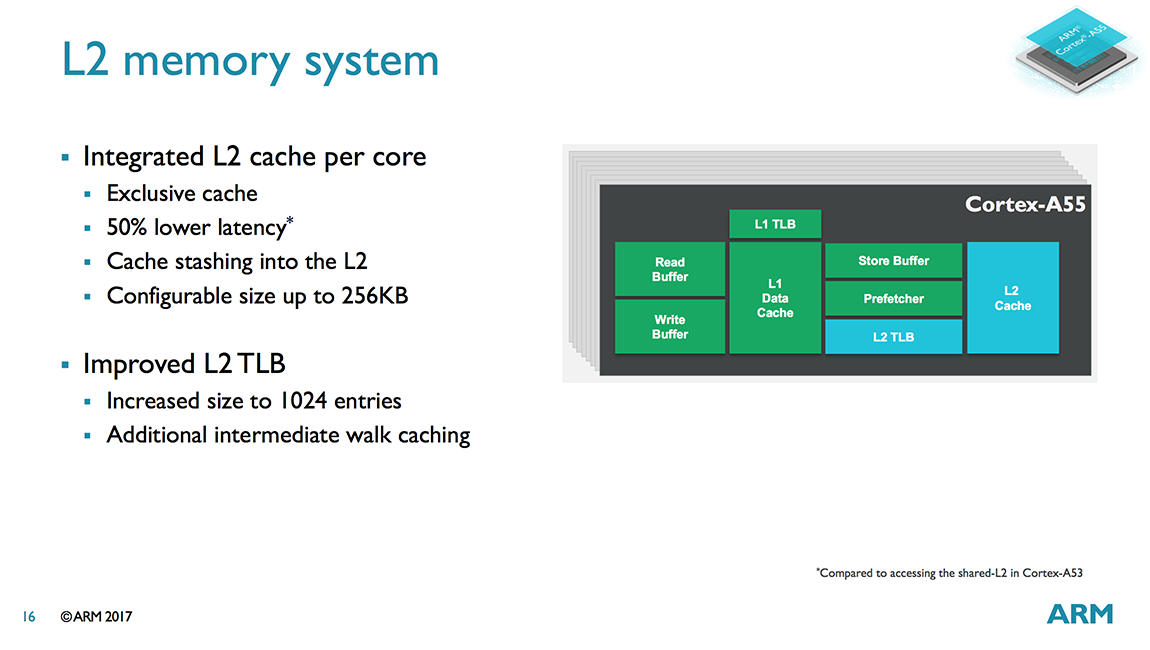
The L2 is 4-way set associative like the L1, a design choice meant to minimize cache latency, which is important for reducing the impact of stalls on in-order cores. The downside to using a less associative cache is a greater chance to miss, but ARM feels comfortable with this compromise with an L3 cache sitting reasonably close to the core.
Having access to a (potentially) large L3 cache, something the A53 did not have, will also help improve performance. As previously stated, in-order cores are sensitive to cache misses that cause the core to stall, so they respond particularly well to increases in cache size and reductions in memory access latency. ARM says the A53/A55 sees roughly a 5% performance improvement for each doubling of cache size depending on workload.
We’ll end our tour through the data path and our discussion about the A55’s memory system improvements with the AGUs (Address Generation Units). According to ARM’s internal benchmarking, the CPU can spend a lot of time doing loads and stores, so improving performance here was crucial. Instead of sticking with the A53’s single, combined AGU, the A55 uses independent load and store AGUs that can perform loads and stores in parallel, enabling a higher issue rate into the memory system. Note that the A55’s AGUs are not capable of performing both loads and stores (just one or the other) like the AGUs in the A73/A75, a trade off between performance and complexity.
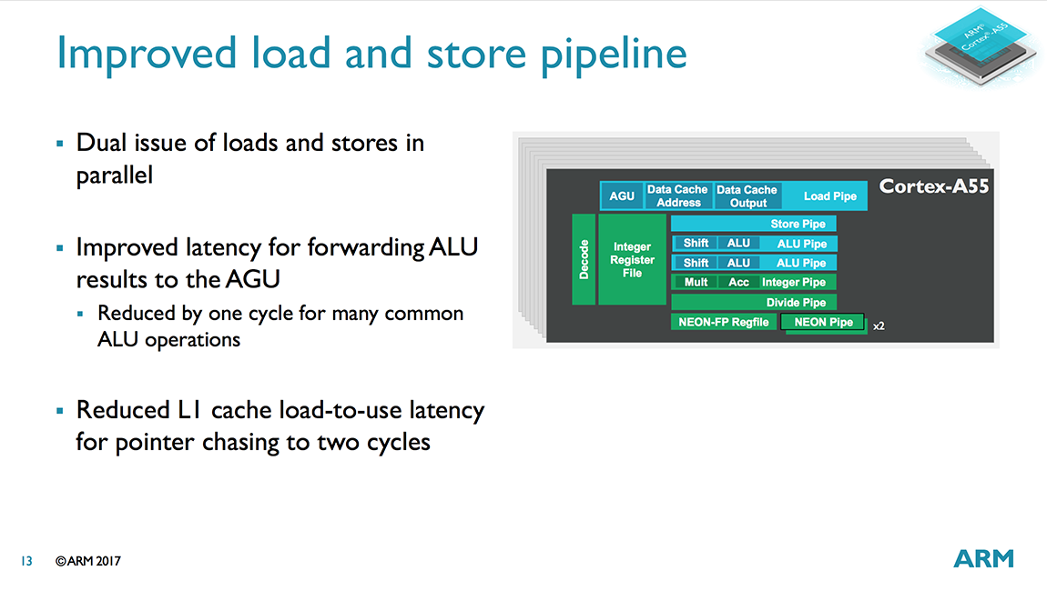
Shifting our focus to the execution pipes, we find 2 ALU/INT units that are functionally the same as the A53’s. Both ALUs can perform basic operations such as additions and shifts, but only one ALU handles integer multiplication and multiply-accumulate operations, while the other focuses on integer division with a Radix-16 divider. So while the A53/A55 cannot perform 2 integer multiplies or divides in parallel, it can dual issue a MUL/MAC alongside a divide/add/shift. The ALUs are still 2 stages, but nearly all instructions complete in 1 cycle. There are also several forwarding paths built in, including paths within the same pipe or cross pipe, to reduce execution latency.
The 2 64-bit NEON/Floating Point pipes are still optional (some markets do not require them) and are served from a dedicated 128-bit register file like the A53. Each SIMD NEON pipe in the A53/A55 can perform 8 8-bit integer, 4 16-bit integer, 2 32-bit integer or single-precision floating-point (FP), or 1 64-bit integer or double-precision FP operations per cycle, giving programmers the flexibility to choose the right balance between precision and performance. As part of its support for the ARMv8.2 architecture, the A55 gains native support for half-precision FP16 operations too. The A53 can fetch FP16 values, but they need to be converted to FP32 before execution. This is no longer the case with A55, so the core performs less work when dealing with FP16 values that are frequently used in some image processing and machine learning applications that require 16-bit precision.
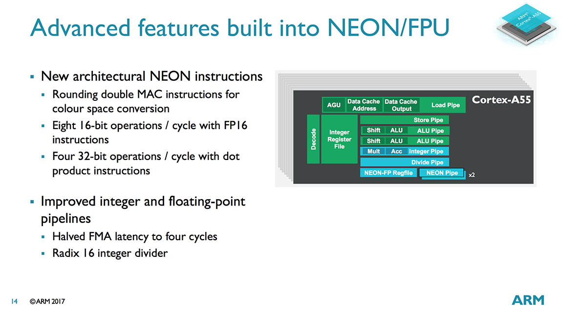
The A55 also includes a new INT8 dot product instruction, another useful addition for machine learning, that offers a 4x performance improvement over the A53 (which increases to about 5x when taking the memory system improvements into account). Instead of executing multiple instructions back to back to back like the A53, the A55 only needs to push a single instruction through the pipe.
One final noteworthy improvement is the ability to do a fused multiply–add (FMA) in a single pass instead of two for the A53, reducing latency from 8 cycles to 4.
The A55 has much in common with the A53, which is not surprising because the A53 already delivers good core throughput. While the A55 gets some improvements to the NEON/FP pipes, mostly from additional instructions courtesy of ARMv8.2, most of its performance gains come from changes to the memory system meant to reduce both the number of core stalls and their latency impact when they do occur.
ARM has certainly been busy, refreshing several key technologies for the next generation of SoCs. DynamIQ might not be as flashy as a new CPU, but as a replacement for big.LITTLE it’s every bit as important. It will be interesting to see how ARM’s partners utilize its flexibility. Will we continue to see the same 4+4 combination of big and little cores at the high end and 8 little cores in the low end to midrange? Or will we see new 7+1 or 3+1 combinations with a single A75 surrounded by A55s? Currently only the A75/A55 are compatible with DynamIQ, and the new CPUs cannot be mixed with older cores using big.LITTLE. This means we will not see the A35 used in mobile outside of MediaTek’s Helio X30.
DynamIQ is an upgrade to bL in other ways too. Placing both the big and little cores inside the same cluster brings several benefits: making the L2 caches local to each CPU and adding an optional L3 cache improves overall memory performance, thread migration latency is reduced, and CPUs can be powered up/down more quickly, which could lead to better battery life.
The A55’s extra performance is a welcome change. This should yield tangible improvements to the user experience in mobile applications, certainly for devices that use A55 cores exclusively. Even devices with A75 cores should still see some benefit considering how threads spend most of their time running on the little cores.
ARM already pushed throughput through the A53’s 2-wide in-order core about as far as it could. Given the power and area targets for A53/A55, going wider or out of order are not possible at this stage. Instead, ARM focused on improving the memory system, reducing latency and improving utilization of the in-order core by keeping it fed with data. The increased performance comes with a small bump in power, but overall efficiency is better.

For the A75, the move to 3-wide decode, improvements throughout the cache hierarchy, and tweaks to improve its out-of-order capability should yield clear performance gains over the A73 in both integer and floating-point workloads. At the same frequency, the A72 actually performs better than A73 in some situations. I expect this will not be the case with A75.
According to ARM’s numbers, the A75’s performance gains help it maintain the same efficiency as the A73, but power consumption is higher, which concerns me a little. ARM has an implementation team optimizing its reference design, so its power numbers are sort of a target for SoC vendors. Because of pressure to reduce time to market, vendors do not always have the same amount of time to optimize their designs, resulting in higher power consumption and lower efficiency. Hopefully, vendors put in the effort to match or get close to ARM’s numbers.
ARM’s primary goal for A72 was reducing power, for A73 it was improving power efficiency, and for A75 it’s improving performance. What will be the goal for the next core, which will be coming from ARM’s Austin team that produced the A72? Will it look similar to A75, or will there be a significant shift in philosophy like we saw with A72 to A73? There is communication and cross pollination of ideas between teams so there’s sure to be some similarities, especially with the execution pipes. The biggest changes should be in the front end, and I would not be surprised to see an extra ALU pipe with the move to 7nm.
If all goes according to plan, we should see the first SoCs using DynamIQ and the A75/A55 in Q1 2018 (maybe Q4 2017) on 10nm.
Autore: Matt Humrick AnandTech