Over the last two weeks, AMD officially launched their 7th Generation Bristol Ridge processors as well as the new AM4 socket and related chipsets. The launch was somewhat muted, as the target for the initial launch is purely to the big system OEMs and system integrators, such as Lenovo, HP, Dell and others – for users wanting to build their own systems, ‘Product-in-Box’ units (called PIBs) for self-build systems will come at the end of the year. We held off on the announcement because the launch and briefings left a number of questions unanswered as to the potential matrix of configurations, specifications of the hardware and how it all connects together. We got a number of answers, so let’s delve in.
The CPUs
The seven APUs and one CPU being launched for OEM systems spans from a high-frequency A12 part using the 7th Generation microarchitecture (we call it Excavator v2) to the A6, and they all build on the Bristol Ridge notebook parts that were launched earlier in the year but focused on the desktop this time around. AMD essentially skipped the 6th Gen, Carrizo, for desktop as the design was significantly mobile focused – we ended up with one CPU, the Athlon X4 845 (which we reviewed), with DDR3 support but no integrated graphics. Using the updated 28nm process from TSMC, AMD was able to tweak the microarchitecture and allow full on APUs for desktops using a similar design.
The full list of processors is as follows:
| AMD 7th Generation Bristol Ridge Processors |
| |
Modules/
Threads |
CPU Base /
Turbo (MHz) |
GPU |
GPU Base /
Turbo (MHz) |
TDP |
| A12-9800 |
2M / 4T |
3800 / 4200 |
Radeon R7 |
800 / 1108 |
65W |
| A12-9800E |
2M / 4T |
3100 / 3800 |
Radeon R7 |
655 / 900 |
35W |
| A10-9700 |
2M / 4T |
3500 / 3800 |
Radeon R7 |
720 / 1029 |
65W |
| A10-9700E |
2M / 4T |
3000 / 3500 |
Radeon R7 |
600 / 847 |
35W |
| A8-9600 |
2M / 4T |
3100 / 3400 |
Radeon R7 |
655 / 900 |
65W |
| A6-9500 |
1M / 2T |
3500 / 3800 |
Radeon R5 |
720 / 1029 |
65W |
| A6-9500E |
1M / 2T |
3000 / 3400 |
Radeon R5 |
576 / 800 |
35W |
| Athlon X4 950 |
2M / 4T |
3500 / 3800 |
– |
– |
65W |
AMD’s mainstream processors will now hit a maximum of 65W in their official thermal design power (TDP), with the launch offering a number of 65W and 35W parts. There is the potential to offer CPUs with a configurable TDP, however much like the older parts that supported 65W/45W modes, it was seldom used, and chances are we will see OEMs stick with the default design power windows here. Also, the naming scheme: any 35W part now has an ‘E’ at the end of the processor name, allowing for easier identification.
As part of this review, we were able to snag a few extra configuration specifications for each of the processors, including the number of streaming processors in each, base GPU frequencies, base Northbridge frequencies (more on the NB later), and confirmation that all the APUs launched will support DDR4-2400 at JEDEC sub-timings.
| AMD 7th Generation 65W Bristol Ridge Processors |
| |
Modules/
Threads |
CPU Base /
Turbo (MHz) |
GPU
SPs |
GPU Base /
Turbo (MHz) |
Northbridge
Base (MHz) |
| A12-9800 |
2M / 4T |
3800 / 4200 |
512 |
800 / 1108 |
1400 |
| A10-9700 |
2M / 4T |
3500 / 3800 |
384 |
720 / 1029 |
1400 |
| A8-9600 |
2M / 4T |
3100 / 3400 |
384 |
655 / 900 |
1300 |
| A6-9500 |
1M / 2T |
3500 / 3800 |
384 |
720 / 1029 |
1400 |
| Athlon X4 950 |
2M / 4T |
3500 / 3800 |
– |
– |
1400 |
| AMD 7th Generation 35W Bristol Ridge Processors |
| |
Modules/
Threads |
CPU Base /
Turbo (MHz) |
GPU
SPs |
GPU Base /
Turbo (MHz) |
Northbridge
Base (MHz) |
| A12-9800E |
2M / 4T |
3100 / 3800 |
512 |
655 / 900 |
1300 |
| A10-9700E |
2M / 4T |
3000 / 3500 |
384 |
600 / 847 |
1300 |
| A6-9500E |
1M / 2T |
3000 / 3400 |
256 |
576 / 800 |
1300 |
The A12-9800 at the top of the stack is an interesting part on paper. If we do a direct comparison with the previous high-end AMD APUs, the A10-7890K, A10-7870K and A10-7860K, a lot of positives end up on the side of the A12.
| High-End AMD APU Comparison |
| |
A12-9800 |
|
A10-7890K |
A10-7870K |
A10-7860K |
|
A10-9600 |
| MSRP |
– |
|
$ 165 |
$ 137 |
$ 117 |
|
– |
| Platform |
Bristol Ridge |
|
Kaveri Refresh |
|
Bristol Ridge |
| uArch |
Excavator v2 |
|
Steamroller |
Steamroller |
Steamroller |
|
Excavator v2 |
| Threads |
2M / 4T |
|
2M / 4T |
2M / 4T |
2M / 4T |
|
2M / 4T |
| CPU Base Freq |
3800 |
|
4100 |
3900 |
3600 |
|
3500 |
| CPU Turbo Freq |
4200 |
|
4300 |
4100 |
4000 |
|
3800 |
| IGP SPs |
512 |
|
512 |
512 |
512 |
|
384 |
| GPU Turbo Freq |
1108 |
|
866 |
866 |
757 |
|
1029 |
| TDP |
65W |
|
95W |
95W |
65W |
|
65W |
| L1-D Cache |
192 KB |
|
192 KB |
192 KB |
192 KB |
|
192 KB |
| L1-I Cache |
128 KB |
|
64 KB |
64 KB |
64 KB |
|
128 KB |
| L2 Cache |
2 MB |
|
4 MB |
4 MB |
4 MB |
|
2 MB |
| DDR Support |
DDR4-2400 |
|
DDR3-2133 |
DDR3-2133 |
DDR3-2133 |
|
DDR4-2400 |
| PCIe 3.0 |
x8 |
|
x16 |
x16 |
x16 |
|
x8 |
| Chipsets |
B350
A320
X/B/A300 |
|
A88X
A78
A68H |
A88X
A78
A68H |
A88X
A78
A68H |
|
B350
A320
X/B/A300 |
The frequency of the A12-9800 gives it a greater dynamic range than the A10-7870K (having 3.8-4.2 GHz, rather than 3.9-4.1), but with the newer Excavator v2 microarchitecture, improved L1 cache, AVX 2.0 support and a much higher integrated graphics frequency (1108 MHz vs. 866 MHz) while also coming in at 30W less TDP. The 30W TDP jump is the most surprising – we’re essentially getting better than the previous A10-class performance at a lower power, which is most likely why they started naming the best APU in the stack an ‘A12’. Basically, the A12-9800 APU will be an extremely interesting one to review given the smaller L2 cache but faster graphics and DDR4 memory.
A Wild Overclocker Appears!
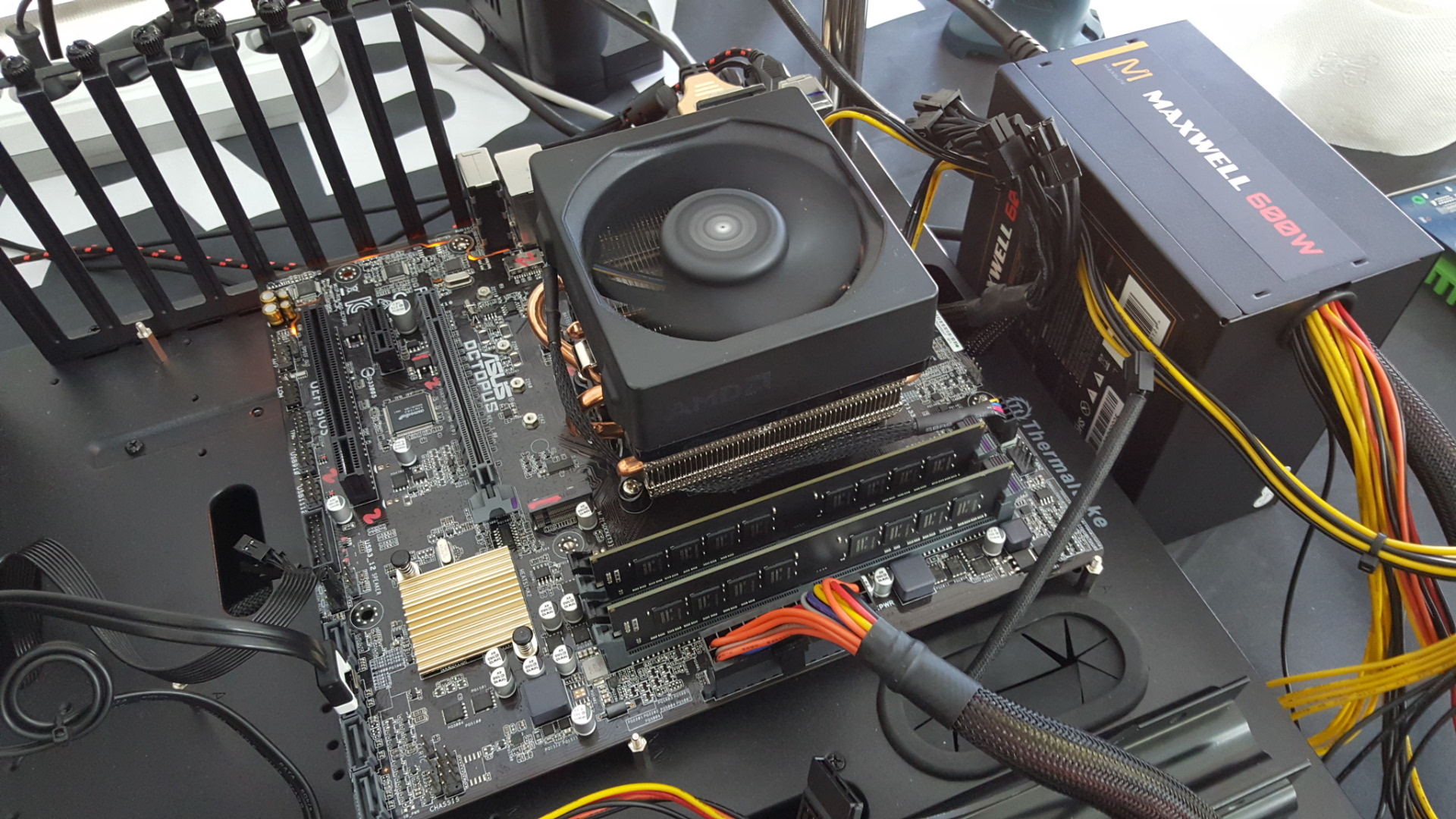
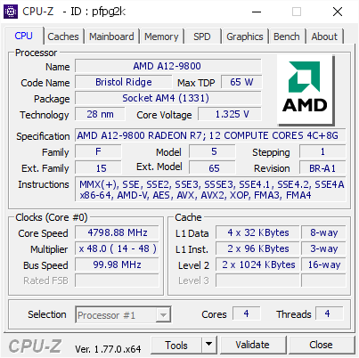
Given that technically the systems with the new APUs have been released for a couple of weeks, some vendors have their internal enthusiasts play around with the platform. Bearing in mind that AMD has not announced any formal overclocking support on these new APUs, NAMEGT, a South Korean overclocker with ties to ASUS, has pushed the A12-9800 APU to 4.8 GHz by adjusting the multiplier. To do this, he used an unreleased ASUS Octopus AM4 motherboard and AMD’s 125W Wraith air cooler (which will presumably be bundled with PIBs later in the product cycle).


Credit: NAMEGT and HWBot
NAMEGT ran this setup on multithreaded Cinebench 11.5 and Cinebench 15, scoring 4.77 and 380 respectively for a 4.8 GHz overclock. If we compare this to our Bench database results, we see the following
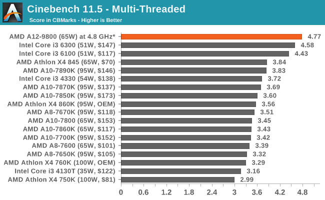
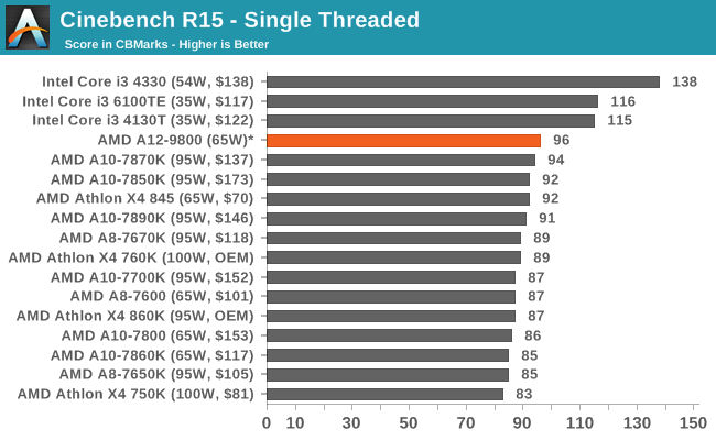
For Cinebench 15, this overclocked score puts the A12-9800 above the Haswell Core i3-4360 and the older AMD FX-4350, but below the newer Skylake i3-6100TE. The Athlon X4 845 at stock frequencies scored 314 while running at 3.5 GHz, which would suggest that a stock A12-9800 at 3.8 GHz would fall around the 340 mark.
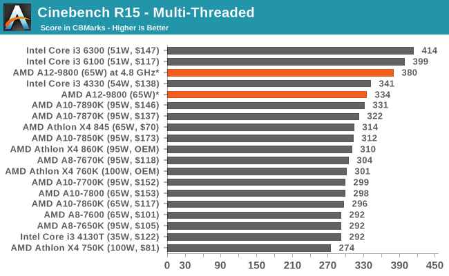
(Since writing this, a preview by Korean website Bodnara, using the A12-9800 in a GIGABYTE motherboard, scored 334 for a stock Cinebench 15 multithreaded test and 96 for the single threaded test. We’ve added this result for perspective.)
When we previously tested the Excavator architecture for desktop on the 65W Athlon X4 845, overclocking was a nightmare, with stability being a large issue. At the time, we suspected that due to the core design being focused towards 15W, moving beyond 65W was perhaps a bit of a stretch for the design at hand. This time around, as we reported before, Bristol Ridge is using an updated 28nm process over Carrizo, which may have a hand in this.
When we asked AMD about overclocking details on the new APUs, the return reply was along the lines of ‘No OEM systems at this time will be unlocked, and no official comment on the individual units. More details will be released closer to the platform launch for DIY users’.
The launch of Bristol Ridge APUs for desktop is taking a slightly different strategy to previous AMD launches. Typically we expect to see CPUs/APUs and OEM systems with that hardware launched on the day of the announcement, with stock of the hardware getting to shelves over the next few weeks. In order to do this, AMD needs to work with all the OEMs (HP, Lenovo, Dell) and platform partners (ASUS, GIGABYTE, MSI, ASRock) and potentially the memory manufacturers (Crucial, Kingston, G.Skill, ADATA, etc) to synchronize a launch with expected hardware, platform control and settings.
This time around, AMD has focused on the OEMs first, with all-in-one PCs and desktop systems being their focus. Typically the big OEMs develop their own PCBs and manage the full gamut of support, as well as being mindful of firmware that can be a work in progress up until the launch date. This allows the launch to be focused on a few models of complete experience systems, rather than the comparative free-for-all with custom build machines. Typically one might argue that the standard motherboard designers take longer to design their product, as it becomes their brand on offer, whereas HP/Lenovo sells the system as a brand, so not every stage has to be promoted, advertised and polished in the same way.
Of course, from an enthusiast perspective, I would prefer everything to come out on day one, and a deep dissection into the platform. But because Bristol Ridge is sharing a platform with the upcoming new microarchitecture, Zen, AMD has to balance the wishes of OEMs along with product expectations. As a result, the base announcement from AMD was somewhat of a brief overview, and we delayed writing this piece until we were able to source certain nuggets of information which make sense when individual units (and motherboards) are on sale for DIY users, as well as some insights into what Zen might offer.
But by focusing on OEMs first, it makes it more difficult for us to source review units! Watch this space, we’re working on it.
The CPU Roadmap
A lot of the recent talk regarding AMD’s future in the desktop CPU space has revolved around its next-generation CPU architecture called Zen. In August, AMD opened up to a significant part of the underlying Zen microarchitecture, detailing a micro-op cache, a layered memory hierarchy, dual schedulers and other information. Nonetheless Zen is initially aiming for the high-end desktop (HEDT) market, and AMD has always stated that Zen will share the AM4 platform with new mainstream CPUs, under the Bristol Ridge and Stoney Ridge names, initially based on an updated Excavator microarchitecture.
AMD’s roadmap seems to be the following:
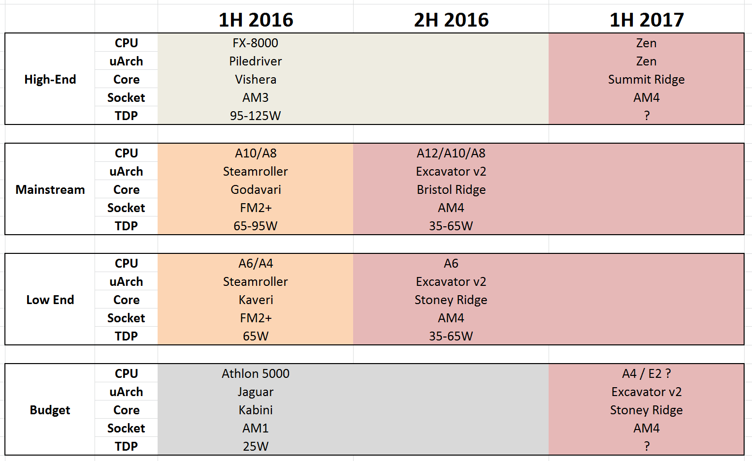
The latest AMD announcements are for that mainstream segment, but we can see that AMD is moving from a three-socket configuration of AM3, FM2+ and AM1 into a singular AM4 platform from top to bottom, with the budget element perhaps being more embedded focused. This has positives and negatives associated with it, which is part of the reason why AMD is staggering the release of Bristol Ridge and the 7th Generation APUs between OEMs and PIBs.
The positive from the unified problem is that AMD’s OEM customers can have a one size fits all solution that spans from the budget to the premium, which makes OEM designs easier to translate from a high powered platform to a budget system. The downside is variety and compatibility – if a vendor designs a platform purely for a budget system, and has fewer safeguards, then a user cannot simply put in the most powerful CPU/APU available. Luckily we are told that all AM4 systems should be dual channel, which migrates away from the Carrizo/Carrizo-L problem we had in notebooks late last year.
For all but one of the processors, integrated graphics is the name of the game. AMD configures the integrated graphics in terms of Compute Units (CUs), with each CU having 64 streaming processors (SPs) using GCN 1.3 (aka GCN 3.0) architecture, the same architecture as found in AMD’s R9 Fury line of GPUs. The lowest processor in the stack, the A6-9500E, will have four CUs for 256 SPs, and the A12 APUs will have eight CUs, for 512 SPs. The other processors will have six CUs for 384 SPs, and in each circumstance the higher TDP processor typically has the higher base and turbo frequency.
| AMD 7th Generation Bristol Ridge Processors |
| |
GPU |
GPU SPs |
GPU Base |
GPU Turbo |
TDP |
| A12-9800 |
Radeon R7 |
512 |
800 |
1108 |
65W |
| A12-9800E |
Radeon R7 |
512 |
655 |
900 |
35W |
| A10-9700 |
Radeon R7 |
384 |
720 |
1029 |
65W |
| A10-9700E |
Radeon R7 |
384 |
600 |
847 |
35W |
| A8-9600 |
Radeon R7 |
384 |
655 |
900 |
65W |
| A6-9500 |
Radeon R5 |
384 |
720 |
1029 |
65W |
| A6-9500E |
Radeon R5 |
256 |
576 |
800 |
35W |
| Athlon X4 950 |
– |
– |
– |
– |
65W |
The new top frequency, 1108 MHz, for the A12-9800 is an interesting element in the discussion. Compared to the previous A10-7890K, we have a +28% increase in raw GPU frequency with the same number of streaming processors, but a lower TDP. This means one of two things – either the 1108 MHz frequency mode is a rare turbo state as the TDP has to be shared between the CPU and APU, or the silicon is sufficient enough to maintain a 28% higher frequency with ease. Obviously, based on the overclocking results seen previously, it might be interesting to see how the GPU might change in frequency without a TDP barrier and with sufficient cooling. For comparison, when we tested the A10-7890K in Grand Theft Auto at a 1280×720 resolution and low-quality settings, we saw an average 55.20 FPS.
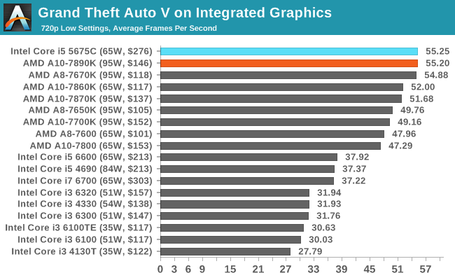
Bearing in mind the change in the cache configuration moving to Bristol Ridge, moving from a 4 MB L2 to a 2 MB L2 but increasing the DRAM compatibility from DDR3-2133 to DDR4-2400, that value should move positive, and distinctly the most cost effective part for gaming.
Each of these processors supports the following display modes:
– DVI, 1920×1200 at 60 Hz
– DisplayPort 1.2a, 4096×2160 at 60 Hz (FreeSync supported)
– HDMI 2.0, 4096×2160 at 60 Hz
– eDP, 2560×1600 at 60 Hz
Technically the processor will support three displays, with any mix of the above. Analog video via VGA can be supported by a DP-to-VGA converter chip on the motherboard or via an external dongle.
For codec support, Bristol Ridge can do the following (natively unless specified):
– MPEG2 Main Profile at High Level (IDCT/VLD)
– MPEG4 Part 2 Advanced Simple Profile at Level 5
– MJPEG 1080p at 60 FPS
– VC1 Simple and Main Profile at High Level (VLD), Advanced Profile at Level 3 (VLD)
– H.264 Constrained Baseline/Main/High/Stereo High Profile at Level 5.2
– HEVC 8-bit Main Profile Decode Only at Level 5.2
– VP9 decode is a hybrid solution via the driver, using CPU and GPU
AMD still continues to support HSA and the arrangement between the Excavator v2 modules in Bristol Ridge and the GCN graphics inside is no different – we still get Full 1.0 specification support. With the added performance, AMD is claiming equal scores for the A12-9800 on PCMark 8 Home with OpenCL acceleration as a Core i5-6500 ($ 192 tray price), and the A12-9800E is listed as a 17% increase in performance over the i5-6500T. With synthetic gaming benchmarks, AMD is claiming 90-100% better performance for the A12 over the i5 competition.
Users keeping tabs on the developments of CPUs will have seen the shift over the last ten years to moving the traditional ‘northbridge’ onto the main CPU die. The northbridge was typically the connectivity hub, allowing the CPU to communicate to the PCIe, DRAM and the Chipset (or Southbridge), and moving this onto the CPU silicon gave better latency, better power characteristics, and reduced the complexity of the motherboard, all for a little extra die area. Typically when we say ‘CPU’ in the context of a modern PC build, this is the image we have, with the CPU containing cores and possibly graphics (which AMD calls an APU).
Typically the CPU/APU has limited connectivity: video outputs (if an integrated GPU is present), a PCIe root complex for the main PCIe lanes, and an additional connectivity pathway to the chipset to enable additional input/output functionality. The chipset uses a one-to-many philosophy, whereby the total bandwidth between the CPU and Chipset may be lower than the total bandwidth of all the functionality coming out of the chipset. Using FIFO buffers, this is typically managed as required. The best analogy for this is that a motorway is not 50 million lanes wide, because not all cars use it at the same time. You only need a few lanes to cater for all but the busiest circumstances.
If the CPU also has the chipset/southbridge built in, either in the silicon or as a multi-chip package, we typically call this an ‘SoC’, or system on chip, as the one unit has all the connectivity needed to fully enable its use. Add on some slots, some power delivery and firmware, then away you go.
Bristol Ridge’s ‘SoC’ Configuration
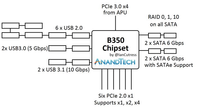
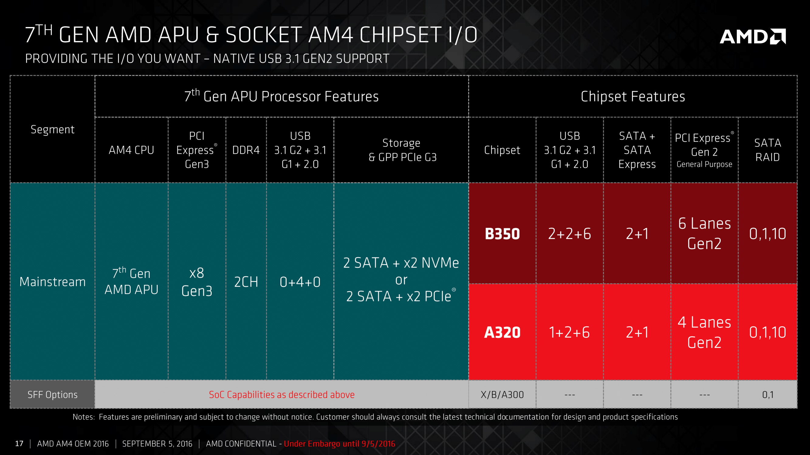
What AMD is doing with Bristol Ridge is a half-way house between a SoC and having a fully external chipset. Some of the connectivity, such as SATA ports, PCIe storage, or PCIe lanes beyond the standard GPU lanes, is built into the processor. These fall under the features of the processor, and for the current launch is a fixed set of features. The CPU also has additional connectivity to an optional chipset which can provide more features, however the use of the chipset is optional.
Here’s a block diagram to help explain:
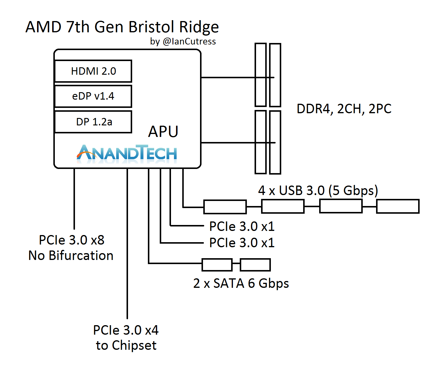
On the APU we have two channels of DDR4, supporting two DIMMs per channel. For the major PCIe devices, we have a PCIe 3.0 x8 port, and this does not support bifurcation (or splitting) to any x4, x2 or x1 combination. It’s a solitary x8 lane suitable for a PCIe x8 port (we’ll discuss what else can be done with this later). The APU communicates with the optional chipset with a PCIe 3.0 x4 link, and we’ve confirmed with AMD that this is a simple PCIe interface. The other parts of the APU give four USB 3.0 ports, two SATA 6 Gbps ports, and two PCIe 3.0 x1 ports. These ports also support NVMe, and can provide two PCIe 3.0 x1 storage ports or can be combined for a single PCIe 3.0 x2.
It Looks Like an x16
Now, if you look at the layout, try counting up how many PCIe lanes are split across all the features. We’ve seen a USB 3.0 hub support four ports of USB 3.0 from a single lane of PCIe 3.0 before, and there are plenty of controllers out there that split a PCIe 3.0 x1 into two SATA ports. So play the adding game: x8 + x4 + x1 + x1 + x1 + x1 = x16. The Bristol Ridge APU seems to suggest it actually has sixteen PCIe 3.0 lanes, but AMD has decided to forcibly split some of them using internal hubs and controllers.
It’s an interesting tactic because it means that systems can be built without a discrete chipset, or the four chipset lanes can be used for other features. However it negates a full PCIe 3.0 x16 link for a full-bandwidth PCIe co-processor. Bearing in mind that if there was a PCIe 3.0 x16 link, there are no additional lanes for a chipset, so there would not be any IO such as SATA ports anyway, such that there would be no physical storage.
The x16 total theory is also somewhat backed up by the lack of bifurcation on the x8 link. Historically a PCIe root complex in a consumer platform that supports x16 can be bifurcated down to x8/x4/x4, and anything else requires additional PCIe switches to support more than three devices. It would seem that AMD has taken the final x4 link and added an on-die PCIe switch to provide those ports, for standard PCIe to USB/SATA controllers. I would hazard a guess and say that what AMD has done is more integrated and complicated than this, in order to keep die area low.
PCIe is Fun with Switches: PLX, Thunderbolt, 10GigE, the Kitchen Sink
Another thing about the x8 link is that it can be combined with an external PCIe switch. In my discussions with AMD, they suggested a switch that bifurcates the x8 to dual x4 interfaces, which could leverage fast PCIe storage while maintaining the onboard graphics for any GPU duties. There’s the other side, in using an x8 to x32 PCIe switch and affording two large x16 links. However, large GPU CrossFire is not one of the main aims for the platform.
Here’s a crazy mockup I thought of, using a $ 100 PCIe switch. I doubt this would come to market.
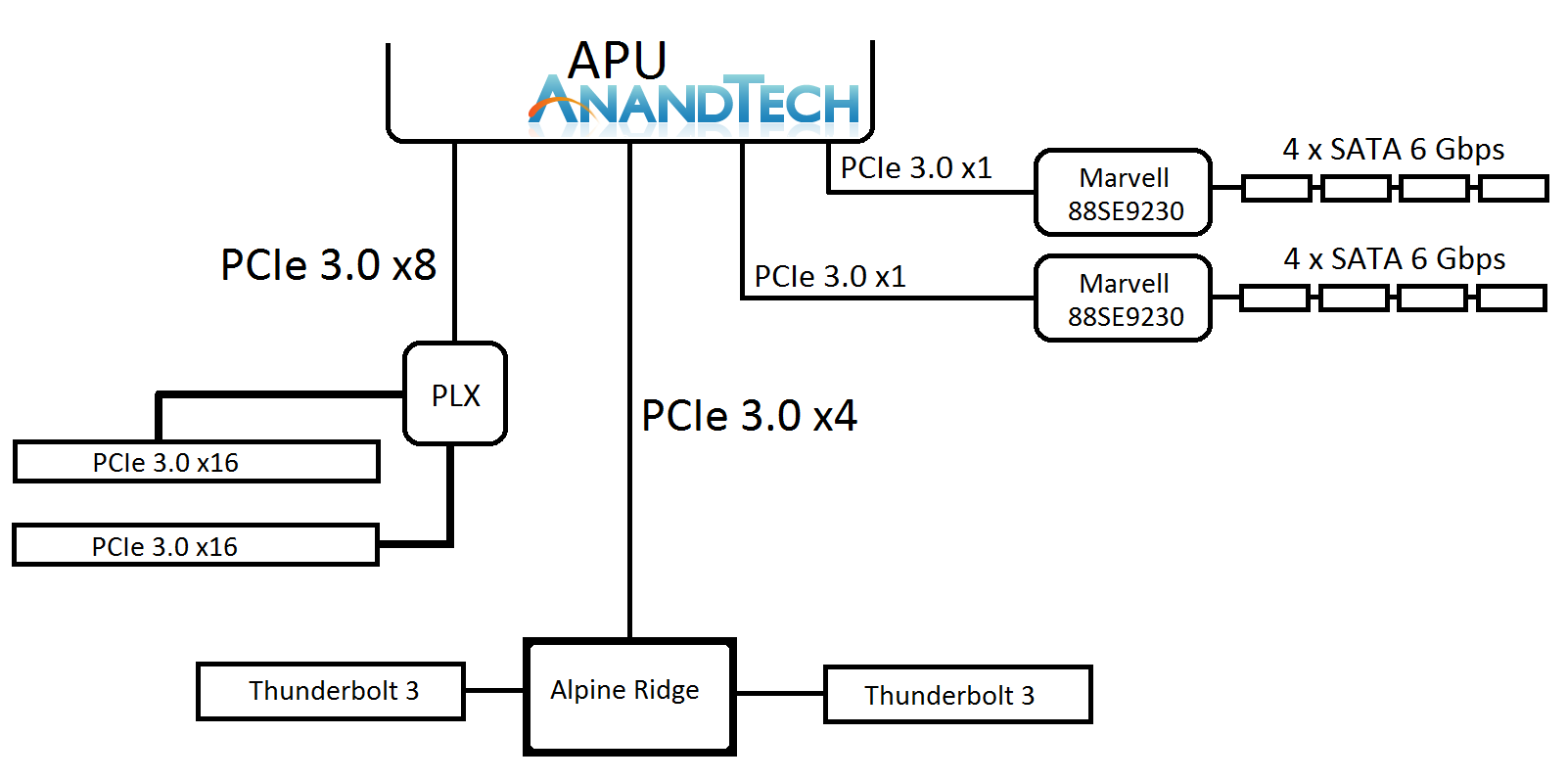
Ian plays a crazy game of PCIe Lego
The joy of PCIe and switches is that it becomes a mix and match game – there’s also the PCIe 3.0 x4 to the chipset. This can be used for non-chipset duties, such as anything that takes PCIe 3.0 x4 like a fast SSD, or potentially Thunderbolt 3. We discussed TB3 support, via Intel’s Alpine Ridge controller, and we were told that the AM4 platform is currently being validated for systems supporting AMD XConnect, which will require Thunderbolt support. AMD did state that they are not willing to speculate on TB3 use, and from my perspective this is because the external GPU feature is what AMD is counting on as being the primary draw for TB3 enabled systems (particularly for OEMs). I suspect the traditional motherboard manufacturers will offer wilder designs, and ASRock likes to throw some spaghetti at the wall, to see what sticks.
Despite all the crazy potential that might come from playing with PCIe, if a user wants more than a couple of SATA ports or x1 slots, the chipset is there to provide. For the Bristol Ridge OEM launch, there are two main chipsets with a further three aimed more at embedded platforms. We’ll focus more on the first two.
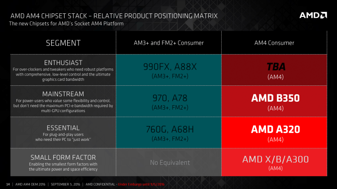
It’s worth noting that AMD has specifically listed that the B350 chipset is not the premium chipset for AM4. We know that Zen will be a part of the AM4 socket and ecosystem, and it would seem that there is at least one specific chipset for the high-end desktop market set to come later. Feel free to speculate.

The B350 and A320 chipsets are mostly identical, using the PCIe 3.0 x4 from the CPU and offering a variety of SATA, USB and PCIe 2.0 connectivity. The PCIe 2.0 lanes, six on the B350 chipset and four on the A320 chipset, support x1, x2 and x4 modes for an array of different controllers. Perhaps the interesting thing here is the support of USB 3.1 at 10 Gbps, which is provided as native support from the chipset.

The main provider of USB 3.1 controllers in the market currently, ASMedia, has been floated around as a partner with AMD in designing these chipsets. We asked AMD if ASMedia was involved, and to what extent, in the development or IP of the hardware. We were told that while the IP is with AMD, ASMedia were bought on as a partner in some fashion (most likely as a design firm or a consultant) to help produce the hardware. We were informed that the chipsets are manufactured at TSMC using a 55nm process, which is a much cheaper process than 28nm or 16nm.
An additional aside, the chipset USB 3.1 ports do not support reversible Type-C natively. We have been informed that a re-driver chip is required to support the revisable connectivity, which is a minor additional IC required by the OEMs.
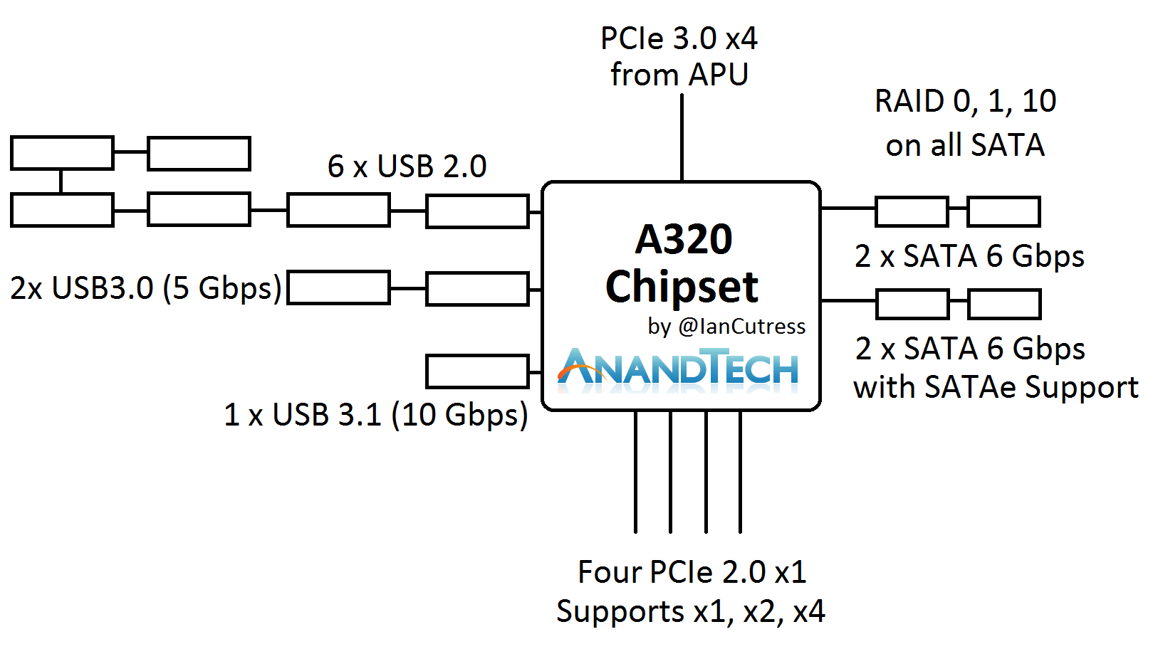
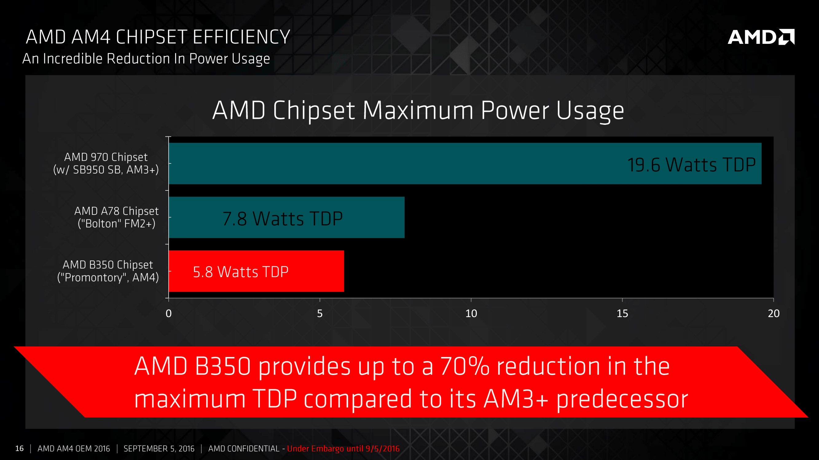
Aside from the native USB 3.1 output, AMD’s chipset offerings are far behind Intel’s current implementation, affording up to 20 PCIe 3.0 lanes from their chipset despite the same uplink equivalent. This is partly because Intel’s chipset has steadily grown and looks more like a PCIe switch itself. AMD is claiming that the external B350 chipset, compared to the older AM3 platforms, comes down from 19.6W TDP to 5.8W TDP.

As an OEM only launch, details about exact systems coming to market (and how they are designed) is providing slim pickings. With a normal retail launch, we have several motherboard manufacturers to dig our teeth into when asking questions, however our relationships with the major OEMs such as HP, Dell or Lenovo are quite different and typically more product focused and less engineering. We’ve not seen any real Bristol Ridge related announcements on OEM systems coming into the market, but some do exist. Reddit user starlightmica saw this HP Pavilion 510-p127c in Costco this week:
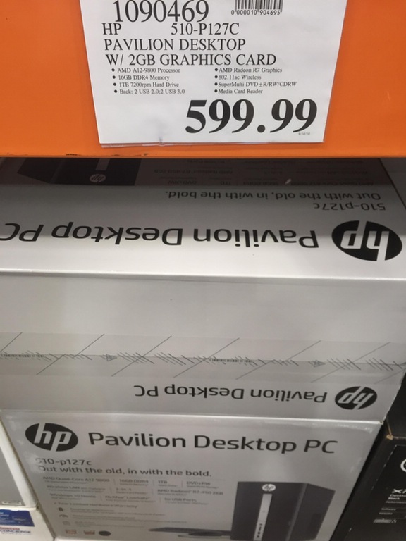
$ 600 gets an A12-9800, 16GB of DDR4, a 1TB mechanical drive, an additional R7 2GB graphics card, 802.11ac WiFi, a DVDRW drive, and a smattering of USB ports (but no USB 3.1, which is interesting).
We reached out to HP, as this system was listed online with the blurriest of motherboard images.
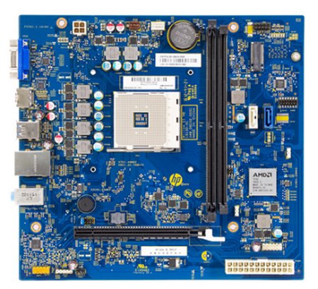
This is a ‘Willow’ motherboard, and we can see the AM4 socket in the middle. Contrary to previous platforms, it is worth noting that the socket mounting holes are significantly more ‘square’ than previous motherboard designs. However, when we discussed the images of the South Korean overclocker near the beginning of this article, it looked like he was using a standard AMD Wraith cooler, which might suggest that this square mounting hole situation might just be HP designing the motherboard.
The board clearly has six phases as part of the power delivery, plus an additional phase for the memory. I would assume that since the system has dual channel support, HP has developed the two memory slots as having dual channel capability, and the abundance of traces from the APU seems to suggest that as well.
To the right of the DRAM slots seems to be a PCIe x1 slot, which is where I assume the WiFi module is held. Below this slot are two of the system SATA ports, followed by what looks like a chipset with a big AMD logo on it and then the 24-pin power connector.
The motherboard has a full PCIe 3.0 x16 sized slot, although as we discussed before, this will be limited to PCIe 3.0 x8 due to the design of the processor. To the left of this is clearly a Realtek audio codec, and judging by the 2.1 support on the rear panel, this is most likely an ALC269 or some other low-end codec. It is hard to tell where the network controller is here without the high-resolution image, but just above and to the left of the speaker looks like a small IC which looks similar to Realtek’s low-end solutions. Typically Realtek offers a deal when audio+networking chips are used in the same system, so I suspect that is what is happening here. Above this are our USB ports, an HDMI output, and a VGA port which must be using a DP-to-VGA IC onboard.
We have closer up images of the socket, thanks to the Hungarian website hwsw:
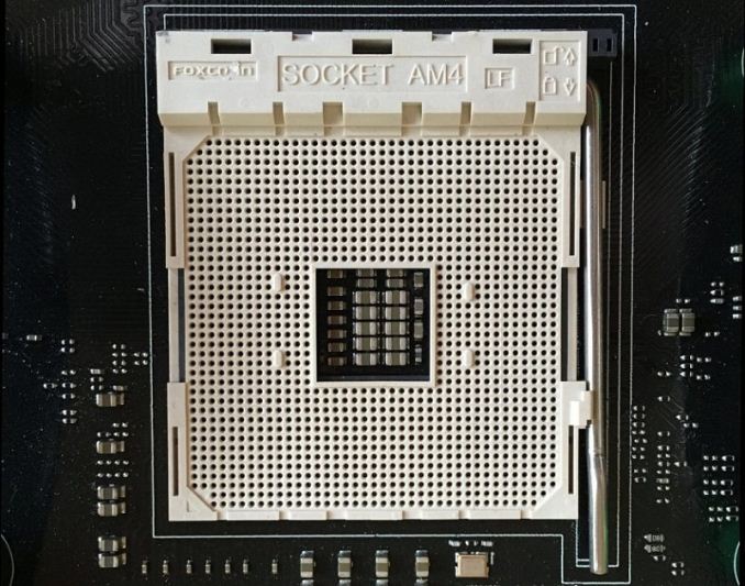
This looks like the standard ZIF socket we’ve come to love/loathe from AMD (I doubt there’s a way that keeps everyone happy anyway), and others have counted 1331 holes which may/may not do things.
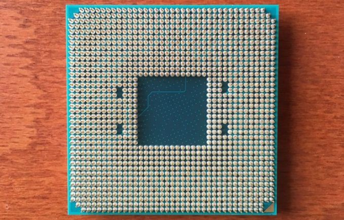
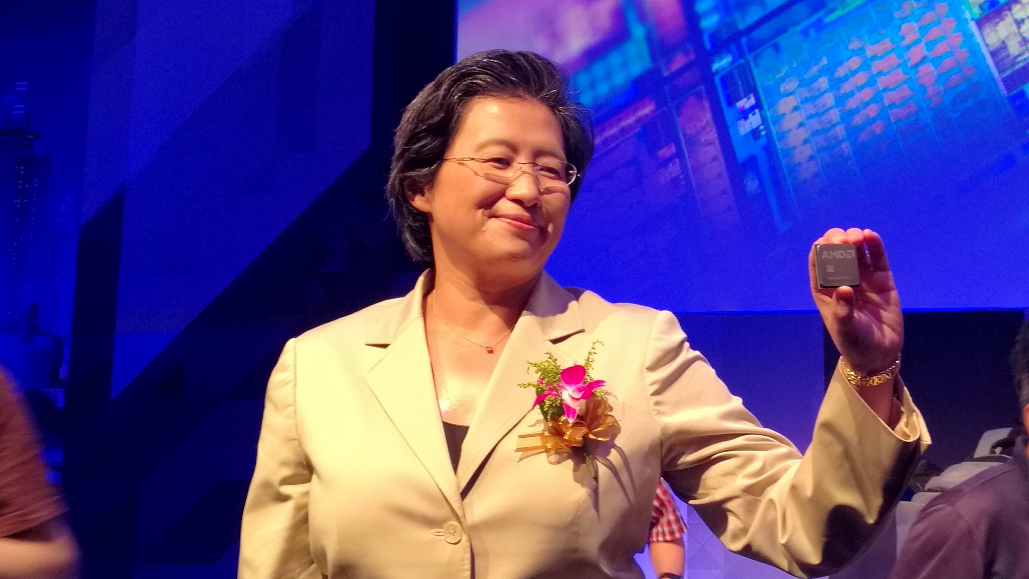
The rear of the CPU, also from hwsw, is what we would expect given the socket layout. It does mean that AMD is stuck at this level of connectivity, to anyone wishing for a quad-channel AMD platform suitable for consumers will have to wait until a future platform. It’s also worth noting that this looks like a similar size to when AMD CEO Lisa Su held up a Zen chip for the press back at the Zen announcements in August.

What Happens Now
Aside from spotting systems like the HP in Costco, no doubt a number of media outlets (us included) are trying to get hold of a number of the APUs for official reviews. As mentioned previously, that A12-9800 looks like an exciting all round part. We are working with AMD to secure the platform and the APUs for testing.
AMD has told us that Bristol Ridge APUs are designed to have price parity with the current Kaveri Refresh/Godavari models, however exact configurations of APUs and coolers, as well as a timeframe for the motherboard manufacturers to come out with their designs, is still to be decided.
I suspect that AMD will wait until closer to the Zen launch window to put Bristol Ridge on the shelves. Attacking the market with a new platform that goes from the high-end desktop through to all but the cheapest systems would mean a concerted effort to gain market share and recognition for catering to the performance needs of as many users as possible all at once. AMD has promised that Zen will trickle down the stack, however as we were told regarding their server and laptop plans later in 2017, that will mostly likely occur later in the year also.
If you’ve read through this piece, or merely skipped to the last page for the conclusions, here’s the take away from the Bristol Ridge for desktop launch:
– OEMs first, DIY builds later
– The A12 at 65W has better specifications than the best previous generation A10 at 95W
– Even at 65W, there is +30% frequency on the integrated graphics for the A12-9800
– The chipsets support USB 3.1 (10 Gbps) natively, but Type-C requires a small additional chip
– Bristol Ridge is more like an SoC, the chipset is entirely optional
– There are so many fun things you can do with PCIe and switches
– We expect the retail APUs to be price drop-ins for current APUs
– We’re trying to get these APUs for review. Stay tuned.


 È un problema? Sì, di immagine. Ma non solo. Perché con questa tempistica significa che alla COP22 l’accordo di Parigi entrerà davvero in vigore. E con l’entrata in vigore si innescano altri meccanismi, importantissimi. A questo punto la questione di immagine si rivela per quello che è: una questione di potere, potere contrattuale. Infatti a Marrakesh, un secondo dopo l’entrata in vigore dell’accordo, verrà creata la “Conference of the Parties serving as the meeting of the Parties to the Paris Agreement”, nome ridondante abbreviato in CMA.