Continuing our Hot Chips 2016 coverage for the evening, along with the requisite presentations on processors, several of the major players in the memory industry are also at the event making their own presentations. A fast chip is only as swift as the memory that is responsible for feeding it, so the development of faster processors is inexorably tied to the development of faster memory technologies and the introduction of additional layers to the computer memory hierarchy.
Like the chip presentations themselves, I should be clear that these aren’t product announcements. But they’re a short, useful look into the challenges the memory manufacturers face and what ideas they’re floating for future generations of memory technology.
Micron
The first memory manufacturer to present was Micron. The firm has an interesting stake in the memory industry; while producing a number of common adopted memory technologies like DDR3 and DDR4, they have also gone their own way in pioneering HBM competitor Hybrid Memory Cube (HMC) and the faster GDDR5X memory technology. The former has not seen much success so far, while the latter has been adopted by NVIDIA for their highest bandwidth configurations on consumer (non-GP100) parts.
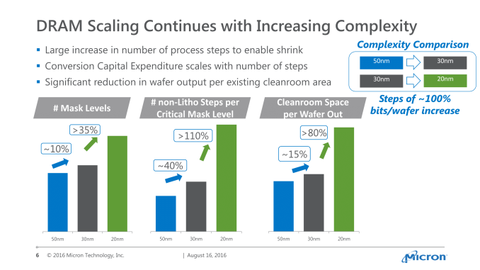
One interesting slide from Micron’s presentation was showing how the memory industry has been impacted by the greater difficultly in manufacturing at smaller geometries. The number of mask levels has increased over the years – especially the number of non-lithographic steps within those mask levels – and meanwhile the total amount of cleanroom space required to hold all of the necessary equipment has similarly increased as well. For an equivalent number of wafers, Micron’s 20nm tech takes more than 80% additional space compared to 30nm, which is not very far off from the 100% increase in memory density that you get from going from 30nm to 20nm in the first place.
The lesson here being that memory manufacturers are facing many of the same constraints as logic manufacturers. Every generation the capital costs increase – and significantly at that – which squeezes margins and investors alike. The memory industry has seen a fairly regular pattern of boom and bust cycles up until now, with each bust cycle claiming a manufacturer or two. However as the number of manufacturers dwindle, I’m not sure consolidation alone is going to be able to continue to offset the higher costs.
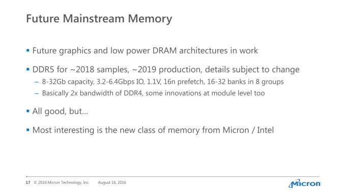
Meanwhile turning towards the future, the company very briefly mentioned their current plan for the memory technology that will follow DDR4, which is aptly being named DDR5. Keeping in mind that the standard has yet to be created and ratified by the JEDEC – and likely won’t be for a couple more years – Micron would essentially like to once again double the DRAM prefetch yet again, to 16n (the same as GDDR5X). Doubling the prefetch doesn’t increase the memory’s internal clock rate, but allows for a larger number of bits to be gathered per clock, and sent out over the higher frequency bus. All the while Micron would also like to get the memory voltage down to 1.1v from today’s 1.2v for standard DDR4.
Presumably this would be using a form of QDR (like GDDR5X), with the current aim to get it into production in 2019.

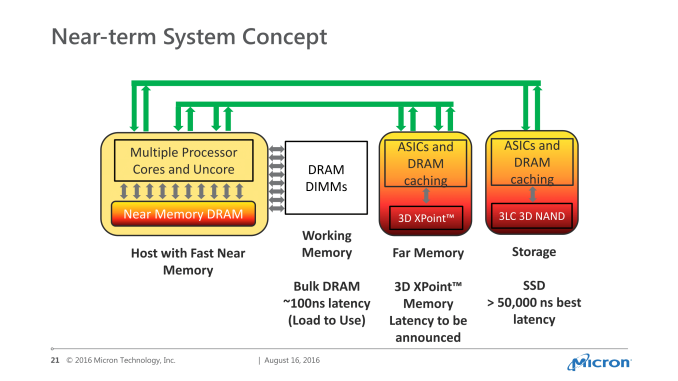
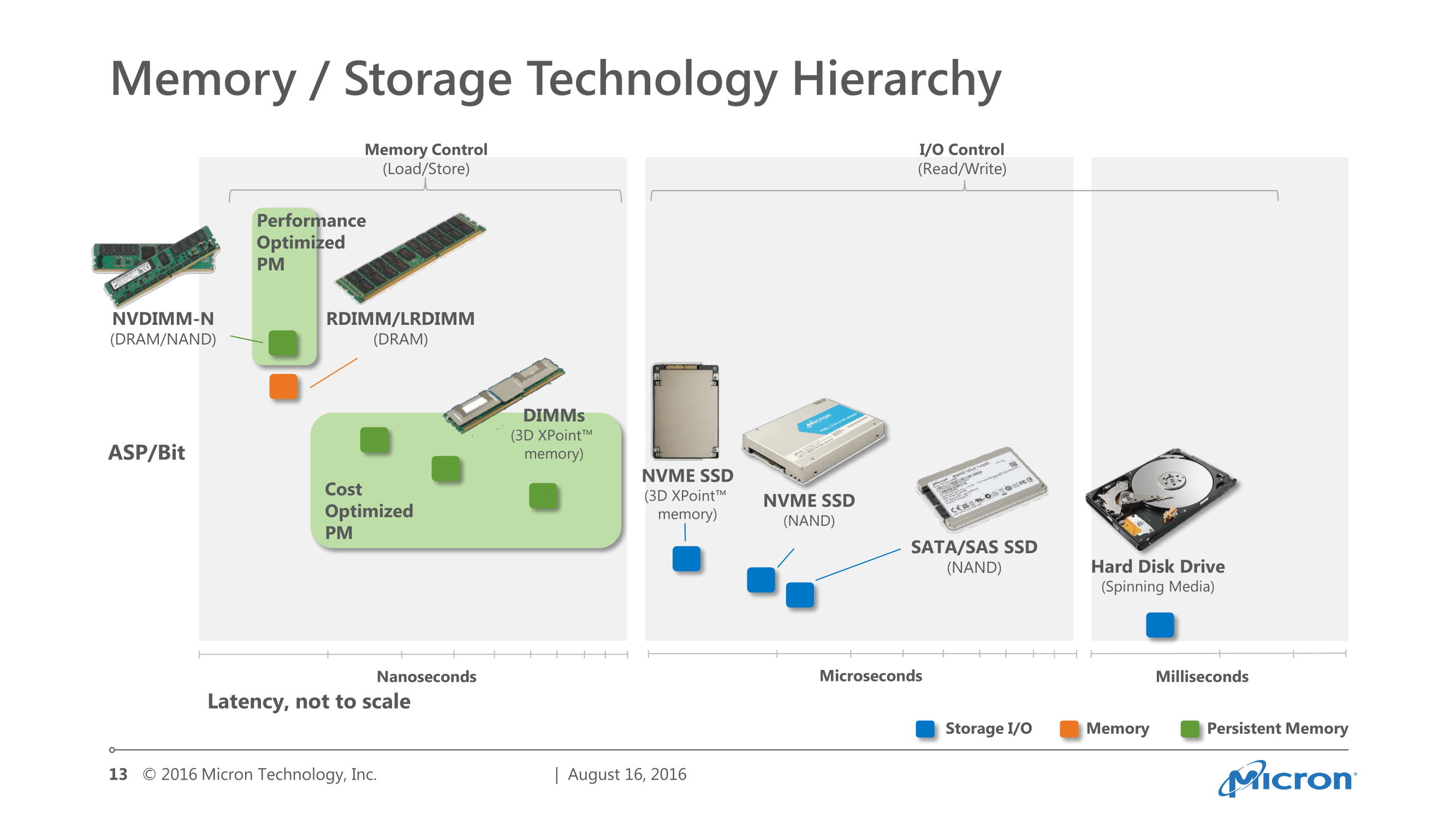
Finally, Micron also published a useful slide that helps to illustrate where they see 3D XPoint memory fitting into the computer memory hierarchy. This is essentially split between SSD-style implementations that access the memory over the PCIe bus, and RAM-style implementations that access the memory over standard memory buses in the form of DIMMs. Neither is as fast as DRAM (and 3D XPoint lacks the near-infinite endurance of DRAM), but it allows for interesting concepts such as databases stored almost entirely in 3D XPoint memory in DIMM form, allowing for relatively fast access combined with the inherent non-volatility of the memory.
Samsung
The second of the memory manufacturers to present was Samsung. Compared to Micron, Samsung has walked the more traditional path, embracing HBM and opting not to build GDDR5X. As a result, in their presentation looking at future memory technologies, we’re seeing where they want to go from today’s HBM2 and GDDR5 technologies.

Throughout their presentation, Samsung laid out ideas for new generation memory standards for DDR, LPDDR, and GDDR5. The bulk of Samsung’s material was on the latter two, focusing their efforts on the realms of high-bandwidth memory technologies and low-power memory technologies.
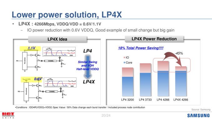
On the low-power side, Samsung is proposing a technology they are calling LP(DDR)4X. An extension of current LPDDR4, Samsung wants to enact changes that allow reducing the memory bus voltage (VDDQ) from 1.1v to 0.6v, nearly halving the voltage required. The end goal would be to further reduce the power consumption of I/O – so not the memory itself, but rather moving data around – which combined with a process node shrink Samsung estimates could reduce total DRAM power consumption by 18%.
As for why Samsung would do this, one needs to look no further than mobile. Power is the ultimate limiting factor of computing performance these days, and that is especially the case on mobile where there is a fixed heat budget and a fixed total power budget in joules. So any reduction in power consumption can either extend battery life, or allow Samsung to further ramp up memory performance at the same power level.

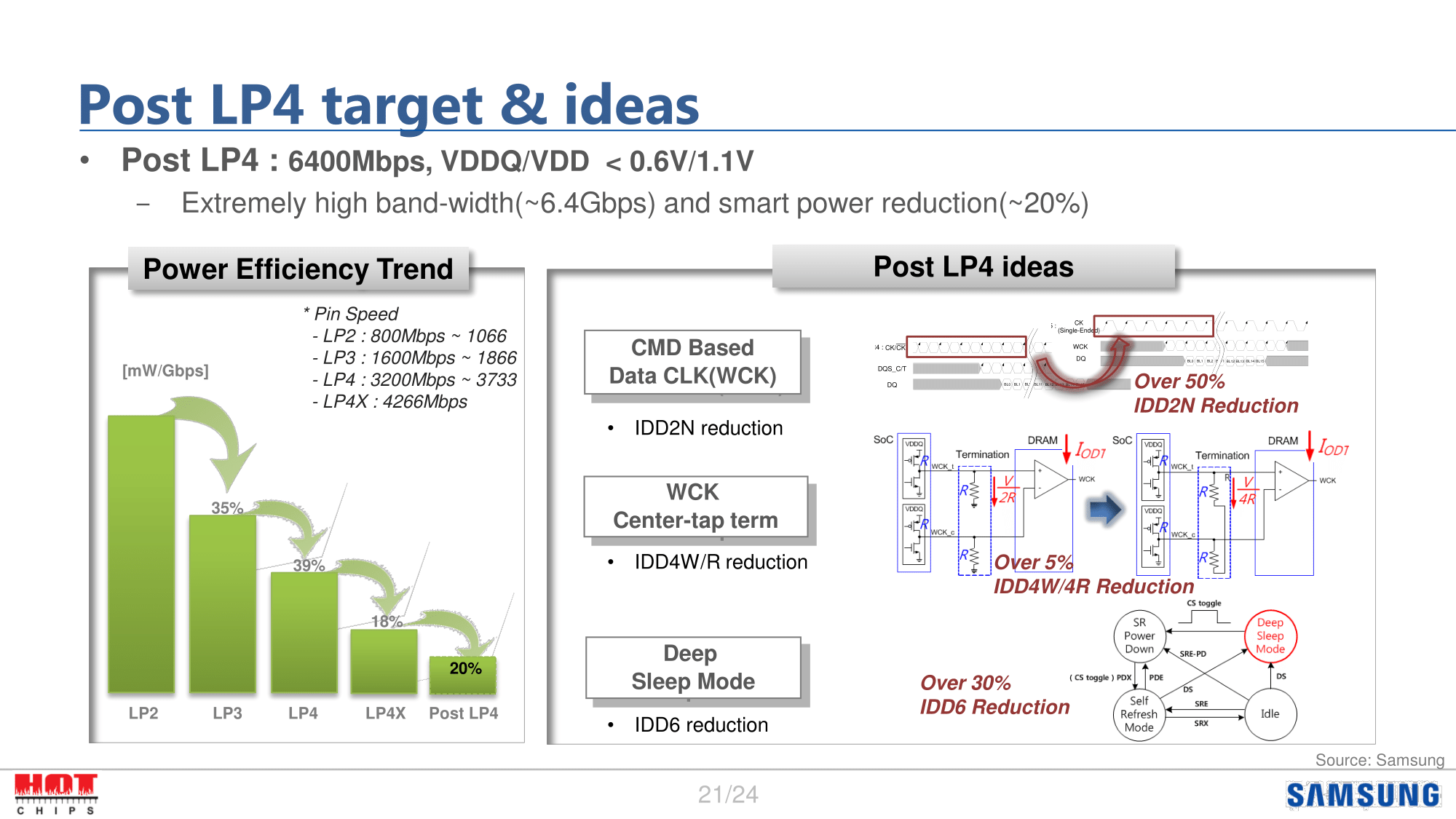
The company also floated some high-level ideas for where they’d like to go with Post LP4 (LPDDR5). Through some optimizations such as even deeper sleep states and adjustments to factors like the precharge standby current, Samsung would like to reduce power consumption per Gbps a further 20% over LP4X.
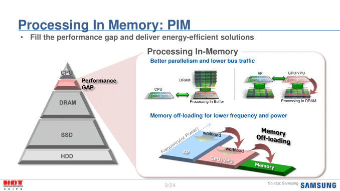

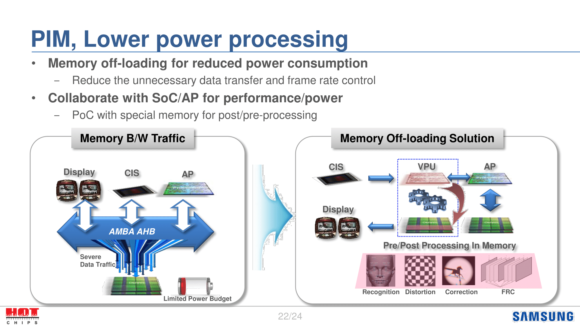
One other idea the company is floating particularly for SoC-type designs is PIM – Processing In Memory. This would move some logic into the DRAM, allowing processing to take place closer to the memory source. The impetus behind this is that I/O power remains one of the biggest components of memory power consumption, and in theory it’s unnecessary since it’s simply moving data rather than processing it or load/storing it. The concept here then would be that by moving some processing closer to DRAM – say parts of a GPU – then less power is spent sending data to the GPU over the expensive memory bus. Instead what’s sent is the already processed data, which is a smaller amount of data, and consequently takes less power to send. The risk, of course, is that you’re now mixing logic with memory, which can be harder to implement and validate.
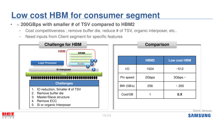
Curiously, Samsung is going almost the opposite direction at the high-end of the memory market. In a proposal for low-cost HBM, Samsung laid out a plan for how to bring down the complexity of HBM, and as a result the total cost of the fast-but-expensive memory technology. The low cost proposal essentially trades off some width for frequency; moving a stack from 1024-bits to 512-bits, but increasing the per-pin frequency by 50%. The net result is still less bandwidth than HBM2, but not immensely so.
The big savings here come from the narrower width allowing for simpler memory stacks with fewer TSVs. TSVs are the breakthrough technology that make HBM possible, but they also remain one of the most stubborn components to get correct, as thousands of vias must be wired up inside a single stack. So a die stack with fewer TSVs will be easier to manufacturer.
The other interesting aspect of this proposal is that Samsung wants to remove the base logic/buffer die. To be honest I’m not 100% sure how this would work, as one of the fundamental tenants of HBM is that it’s a logic-to-logic (processor to logic die) connection, with the HBM stack’s logic die then coordinating the relatively dumb DRAM layers. Removing the logic die would certainly bring down costs, as it means no longer meshing logic with DRAM on a single package, but it’s not clear where the HBM PHY lies on the cost-reduced memory stack.
Finally, partially as a consequence of the narrower I/O, Samsung wants to try to get away from silicon interposers and use organic interposers instead. Silicon interposers are simple – there’s no logic, just routing – but they’re a big chunk of silicon, and that comes at a cost. If they were able to move to an organic interposer, then the interposer cost would be significantly reduced.
Bear in mind that all of this is just a proposal – Samsung’s slide even notes that they still need client feedback to figure all of this out – but it will be interesting to see how much of this gains traction. At the same time I’m left to wonder what the resulting power cost may be; part of what makes HBM so efficient is that it’s wide and slow. The low-cost proposal here makes HBM a little more GDDR-like, and that could sacrifice some of the efficiency improvements.

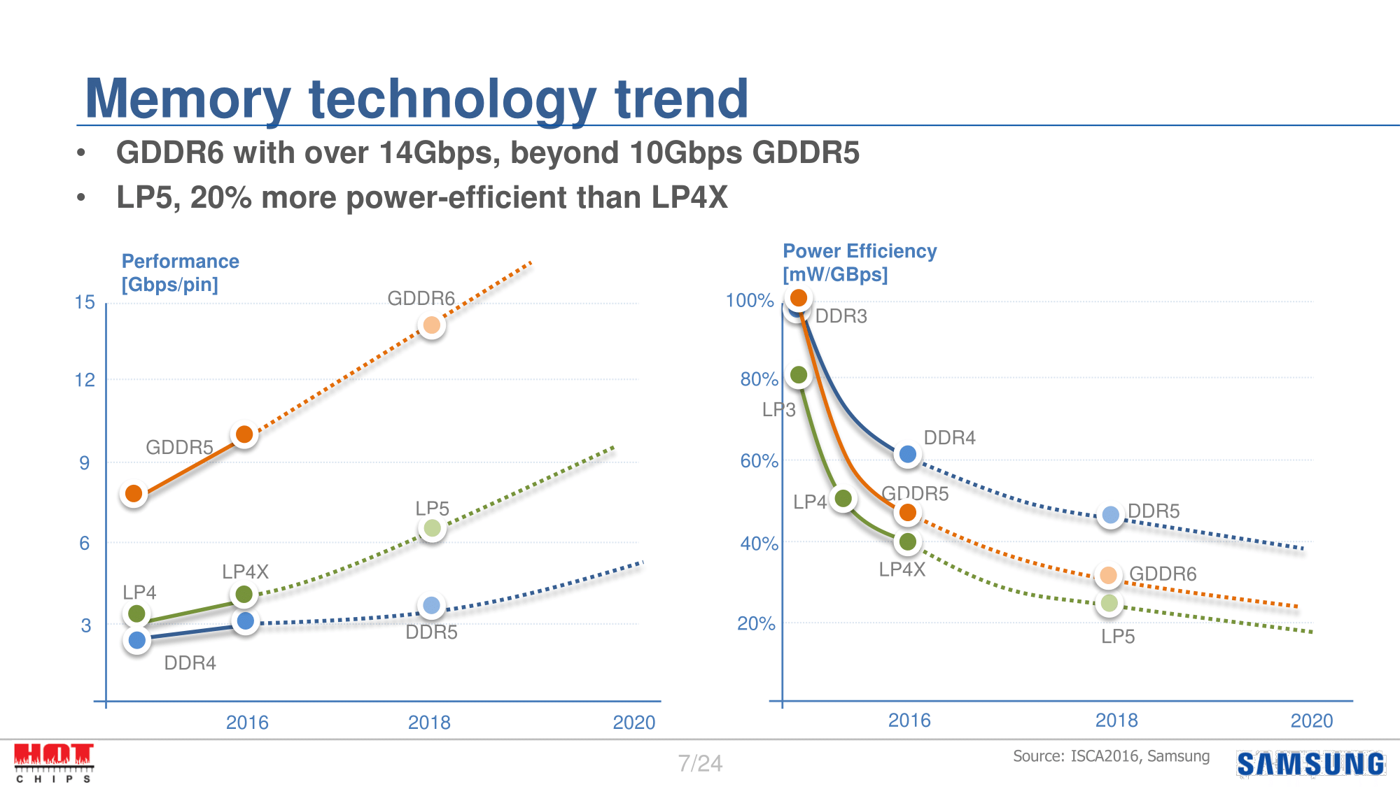
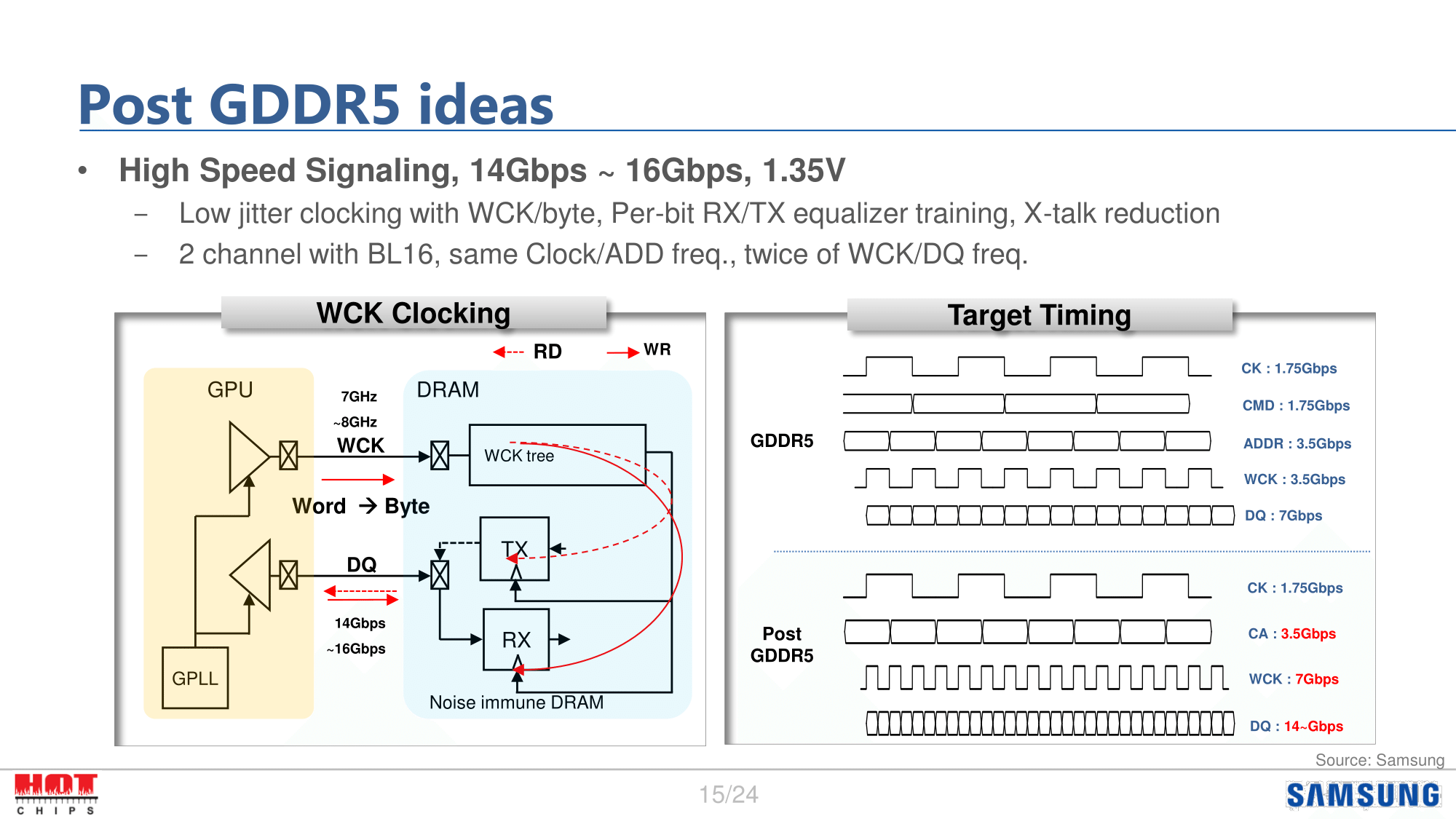
Speaking of GDDR, Samsung also pitched their idea for what Post GDDR5 (GDDR6) would look like. Fundamentally I’m not sure this is all that different from GDDR5X; the memory clock stays the same, while the data clock is doubled versus GDDR5, implying a 16n prefetch. Samsung’s target bandwidth range is from 14 to 16Gbps, which is at the very high end of Micron’s own goals for GDDR5X. I assume there’s more to this than simply a larger prefetch and a faster bus, but we’ll have to see what happens as the manufacturers eventually bring a GDDR6 standard to the market.
SK Hynix
As the memory manufacturer the most responsible for the development of HBM in the first place, SK Hynix’s Hot Chips presentation was all about HBM, its uses, and how technology developed from it can be used in other applications. There’s admittedly very little forward-looking about their presentation – the bulk of it was about why HBM is such a good fit for various applications and how they ensure reliability of the complex technology – but there was a brief discussion of where they want to go for HBM3.
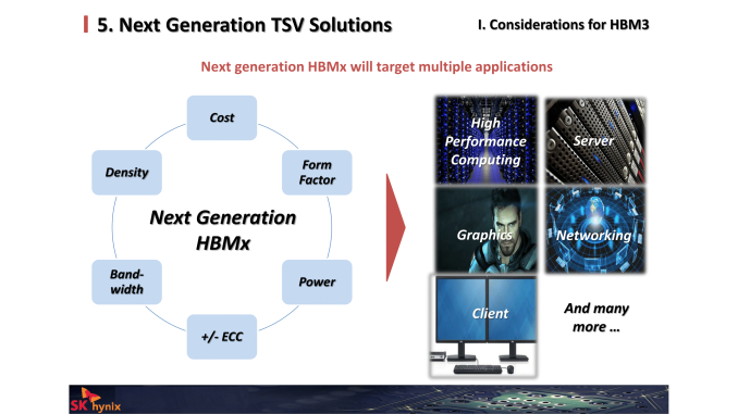
The goal for HBM3 is to broaden its reach from high-end applications of today to a wider range of applications for tomorrow. No specific technologies or changes are proposed in SK Hynix’s slides, but at a high level it’s not too different from Samsung’s low-cost HBM proposal. Specifically, SK Hynix wants to make ECC an optional feature, and they want to make further changes to work on the cost and density of the technology. And of course, they also want to further improve on bandwidth, making HBM even faster at the high-end for the current types of devices that are already using HBM.
Xilinx
The last memory presentation I’ll be coving is from Xilinx. The firm is better known for their FPGAs and other forms of programmable logic, but they are also a major consumer of memory technologies and have their own ideas and concerns for how the memory ecosystem should advance.

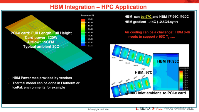
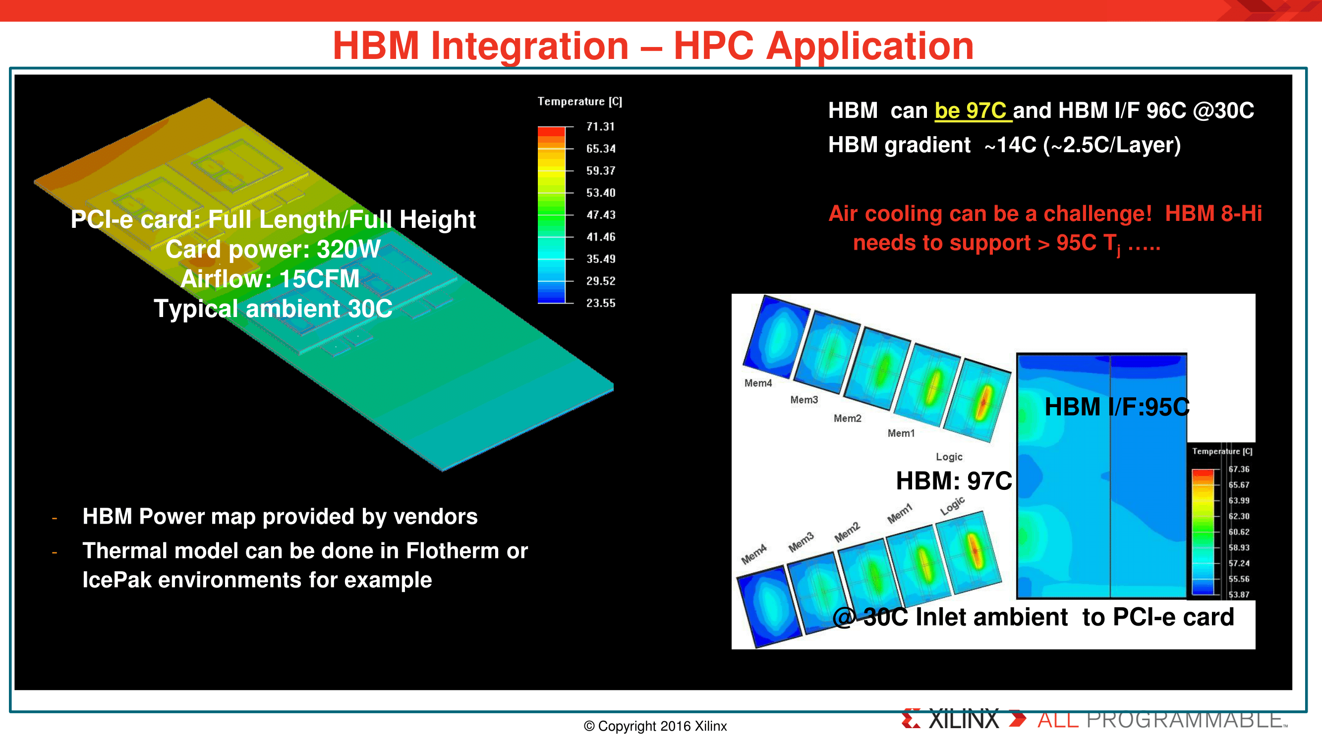
One interesting point made by Xilinx in their presentation was that, as you’d expect for stacking components, heat is an issue. The farther down the stack you go, the warmer it gets. Besides the absolute heat concerns – exceeding a safe temperate for the HBM stack – the fact that the different layers of the memory are running at different temperatures is also less than ideal (think temperature compensation and material expansion).
Xilinx is especially concerned here for what this means for 8-Hi stacks, which double the capacity of an HBM stack by doubling the number of DRAM layers. In practice this would make the lower DRAM and logic layers even more insulated, making them even hotter. And the sheer density of HBM (even an 8-Hi stack isn’t all that tall) makes those lower layers difficult to cool with air. As a result Xilinx is pushing for HBM to be developed so that it can withstand high Tjunction (Tj) temperatures, in order to ensure that air cooling of 8-Hi stacks is viable. To that end, Xilinx would like HBM’s TjMax to be over 95C, which is not an uncommon max temperature (GPUs and CPUs often have similar rules), but none the less illustrates how hot HBM can get.

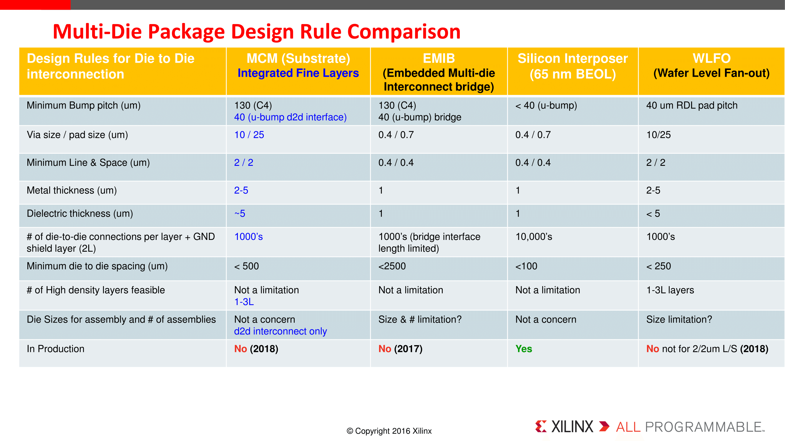
Meanwhile their presentation also contains a handy chart of design rule comparisons for multi-die packaging. This is specifically useful for HBM, as the principles here will be useful for bringing HBM costs down. The silicon interposer is currently the only working option, but like the other presenters, Xilinx would like to have cheaper options in order to broaden the adoption of HBM. If all goes well, technologies like organic substrates and Wafer Level Fan Out may be two such solutions to the problem.