Categorie
HardwareSoftware

Nvidia Titan V, niente supporto a SLI e NVLink

Author: Manolo De Agostini Tom’s Hardware

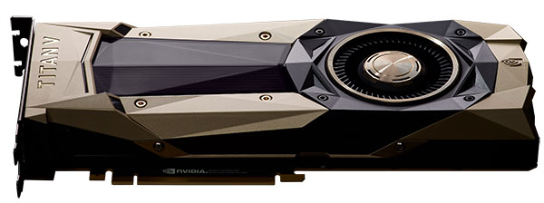
Dopo aver annunciato la Titan V con GPU Volta GV100 un po’ a sorpresa, Nvidia chiarito alcuni punti di questa scheda da 3000 dollari. Si tratta di un acceleratore indirizzato a ricercatori e scienziati che hanno bisogno di un’elevata potenza di calcolo per il loro lavoro, in particolare compiti legati all’intelligenza artificiale, ma non possono affrontare i costi di una Tesla V100.

Proprio per il suo particolare indirizzo, la scheda perde due funzionalità tipiche di altre proposte dell’azienda: la tecnologia multi-GPU SLI e il collegamento NVLink. Non sarà quindi possibile mettere più soluzioni Titan V in parallelo.

pcb nvidia titan v

Per quanto concerne il collegamento ad alta velocità NVLink, non è supportato e probabilmente nemmeno accessibile. La scheda ha due connettori, come si può vedere dalla foto del PCB distribuita da Nvidia, ma si tratta di “rimasugli” della Tesla V100.

D’altronde è inutile creare un circuito stampato diverso per una scheda di cui non saranno poi prodotte tantissime unità. NVLink garantisce comunicazioni tra CPU e GPU, nonché tra le GPU, con velocità da 5 a 10 volte superiori rispetto al tradizionale PCIe 3.0.

nvidia nvlink

Tali connettori, oltre a essere verosimilmente disattivati, sono ostruiti dalla copertura e dai componenti del sistema di raffreddamento, che impediscono il collegamento di qualsivoglia bridge. Sullo store statunitense di Nvidia esiste infatti un bridge NVLink, ma costa 600 dollari ed è pensato per altri prodotti.


Tom’s Consiglia

In attesa di nuove schede video GeForce, la più potente del reame rimane la GTX 1080 Ti. Esiste anche la versione mini.

Categorie
HardwareSoftware

How Snapdragon 845 snaps 25 to 30 percent faster

Author: fudo [AT] fudzilla [DOT] com (Fuad Abazovic) Fudzilla.com – Home

From the horse’s mouth

We know that Qualcomm has officially released the Snapdragon 845 but our key question is how the company managed to get a 30 percent performance increase using the same manufacturing process.

OK, we do know that this is the second generation 10nm process from Samsung that definitely had some smaller impact on the SoC performance. Samsung calls this manufacturing process 10LPP (Low Power Plus) and Qualcomm executives confirmed that this created a minor improvement on general SoC performance.

Alex Katouzian, SVP at Qualcomm, confirmed to Fudzilla that the 30 percent performance increase comes mostly from the new architecture. Tim Leland, the VP that runs Adreno graphics for Qualcomm, also confirmed that the Adreno 630 was designed from the ground up and this is how it managed to save as much as 30 percent of power with 30 percent higher performance.

845pack

The CPU performance grows from the combination of the improved Cortex A75 / Cortex A55 cores and the shared L3 cache memory. From the early days of CPUs and GPUs, Level 3 shared cache was a great way to save a lot of performance and energy. Cortex A55 like designs of smaller cores got us excited when they were announced. Back at Computex 2017, we had a chance to chat with the then President of ARM, Rene Haas, and got a clear answer thatn Cortex A55 can score 50 percent faster than its A53 predecessor, simply as this was because of popular demand by customers. You can run so many workloads on a smaller core and save a lot of energy. This results in a  direct performance increase as well as better battery life of the overall SoC. 

The new architecture

Transferring data from  fast Cortex A75 cores to power optimized Kryo 385 (Cortex A55) is expensive, and it costs you a lot in terms of  power and performance. With L3 cache, this process gets more acceptable and you can save significant data in the L3 – and save the SoC from expensive memory writes.

Qualcomm calls the Snapdragon 845 CPU component the Kryo 385 as it made changes to the pipeline and the Cortex A75 core itself. This is the only way to stay ahead of the competition without needing to design the CPU core from the ground up.

Kryo385

Adreno 630 is also up to 30 percent faster with 30 percent less power consumption that will give better gaming performance as well as supporting the newer VR, AR and XR.  technologies.

Well this is all Qualcomm. It’s always a better choice than licensing widely available and reliable graphics like Mali from ARM or PowerVR from Imagination Technologies. At the same time, developing the GPU from the ground up takes a lot of software and hardware skills and it is expensive, but with a great team it gets you to the best possible final score.  

Categorie
HardwareSoftware

Adreno 630 runs console like game at 1080

Author: fudo [AT] fudzilla [DOT] com (Fuad Abazovic) Fudzilla.com – Home

Lineage 2 Revolution does not throttle

We had a chance to see a Snapdragon 845 prototype phone factor design running Lineage 2 revolution 1080p 60 FPS, in so-called console like gaming.

Lineage 2 Revolution is a mobile MMORPG game licensed by NCSoft and developed by Netmarble and it traditionally runs in 720p resolution on nearly all of the phones available today. This includes Snapdragon 835 phones and the rest of the competition. The Lineage 2 Revolution is an Unreal Engine based game.

In early 2018, you can expect to see Snapdragon 845 phones running it. We had a few minutes to play this graphically impressive MMORPG and we saw with the device is that the reference phone didn’t get hot, nor throttled.

160,000 triangles per frame

The game supports advanced effects including physically based rendering, bloom, dynamic reflection and shadows. Of course, this is all running on the latest lower level API, the well known Vulkan. If you want a few more details, we are talking about 160,000 triangles per frame at 60 frames per second and 10 surfaces per frame.    

adreno630game

This is a big deal, as Qualcomm claims a 25 percent higher performance in games with 30 percent better efficiency. Back in early 2017, when we had a chance to see the first Snapdragon 820 reference phones, we were surprised that they would not throttle or get hot either.

This will play a big role in the slot in VR designs as no one really likes a hot phone  close to your brain.

When we say console like graphics, bear in mind that most games on Xbox One and PlayStation 4 run at 720, but with some higher polygons and better looking games. Still, in the phone form factor, the game looks quite amazing, considering that the consoles have much bigger GPUs and a lot of space to place a bigger cooler, compared to an Adreno 630 GPU inside the few mm thick phone.

Categorie
HardwareSoftware

Toshiba settles with Western Digital

Author: edfu777 [AT] hotmail [DOT] com (Nick Farrell) Fudzilla.com – Home

Deal made, peace pipe to be smoked

Toshiba and Western Digital have agreed in principle to settle a dispute over the Japanese firm’s plans to sell its $ 18 billion chip unit and aim to have a final agreement in place next week.

Word on the street is that the Toshiba board has approved a framework for a settlement.

Western Digital had been able to block a deal to selling the unit to a Bain Capital-led consortium.

The settlement under discussion calls for Western Digital to drop arbitration claims seeking to stop the sale in exchange for Toshiba allowing it to invest in a new production line for advanced flash memory chips that will start next year.

A Toshiba spokesman said that while the company was open to a settlement, it would not disclose discussion specifics or details of board of directors meetings. “It is not a fact that we have reached an agreement with Western Digital”, he said.

Western Digital is not saying anything.

Toshiba was forced to put the unit – the world’s no.2 producer of NAND chips – on the block to cover billions of dollars in liabilities arising from its now bankrupt US nuclear power unit Westinghouse.

The deal with the Bain-led consortium will, however, see it reinvest in the unit and together with Hoya, a maker of parts for chip devices, Japanese firms will hold more than 50 percent of the business – a keen wish of the Japanese government.

As part of the planned settlement, Toshiba and Western Digital would extend existing agreements for their chip joint ventures in Yokkaichi, central Japan, one of the sources said. The current agreements are set to start expiring from 2021.

Western Digital would also invest in a completely new chip plant that Toshiba will start building next year in northern Japan, the source said.

Western Digital, one of world’s leading makers of hard disk drives, paid some $ 16 billion last year to acquire SanDisk, Toshiba’s chip joint venture partner since 2000.

With data storage key to most next-generation technologies from artificial intelligence and autonomous driving to the Internet of Things, NAND chips have only grown in importance and Western Digital has been desperate to keep the business out of the hands of rival chipmakers.

The sale still needs to clear the snarling mauls of the regulatory watchdogs but they are not expected to rip the trousers off the deal.

Categorie
HardwareSoftware

Niente supporto SLI per le schede NVIDIA Titan V

Author: Le news di Hardware Upgrade

Abbiamo segnalato, con questa notizia, l’annuncio della nuova scheda video NVIDIA Titan V quale proposta top di gamma dell’azienda americana nel settore delle schede desktop. Basata su architettura Volta, con GPU GV100, questa scheda integra 12 Gbytes di memoria video di tipo HBM2 e vanta sulla carta le migliori specifiche tecniche tra le schede desktop attualmente disponibili sul mercato.

nvidia-titan_v_2.jpg

NVIDIA ha avviato da quest’oggi le vendite di questo prodotto, che in Italia può essere acquistato a un listino di 3.100€ IVA inclusa. Questa scheda non integra nella parte superiore del PCB i connettori SLI, pertanto non supporta questa tecnologia. La scheda Titan V non può quindi venir utilizzata in configurazioni con due schede installate e utilizzate in parallelo per applicaizoni videoludiche sfruttando tecnologia SLI; questo invece permette di utilizzare due o più di queste schede per elaborazioni parallele che non siano di tipo grafico.

nvidia-titan_v_3.jpg

Tale scelta è molto interessante in quanto conferma il progressivo abbandono al supporto a configurazioni multi-GPU da parte tanto di NVIDIA come di AMD. Tale direzione è ben più spinta nella prima, che da tempo ha ufficialmente accantonato il supporto a configurazioni SLI con più di 2 GPU in parallelo per via della scarsa diffusione e della difficoltà nell’ottenere elevata scalabilità delle prestazioni con la maggior parte dei titoli. AMD continua a supportare configurazioni CrossFireX sino a 4 GPU in parallelo ma la diffusione di sistemi di questo tipo è complessivamente così circoscritta da domandarsi se i costi di ottimizzazione dei driver siano in qualche modo ripagati.

L’assenza di supporto SLI lascia meglio capire come questa scheda sia destinata non tanto al pubblico dei giocatori, in primo luogo per il costo, quanto a quello dei ricercatori e di chi necessita di una scheda potente per il calcolo parallelo ma non ha accesso per budget alle proposte della famiglia Tesla. Titan V, però integra al proprio interno tutto quello che serve per assicurare un’esperienza di gioco ai massimi livelli.