
Perché i principali operatori mobili nell’ultimo anno hanno aumentato le tariffe e sono passati alla fatturazione a 28 giorni? Difficile dare un’unica risposta, certo è che nell’ultimo bollettino AGCOM
Categoria: HardwareSoftware
Categorie
Cisco releases a smartboard
$ 4,990 with a $ 199 monthly subscription for a giant tablet
Cisco is pushing a new “smart” whiteboard to the market with a $ 4,990 price tag and a $ 199 monthly subscription.
The entry level technology appears to be a 55-inch tablet which is screwed to the wall. The company is billing it as a high-tech whiteboard, allowing you to doodle on its canvas, or on a sharp PDF document.
Dubbed the Spark it comes with some video calling tech a 4K camera and display resolution which allows the board to zoom in and out automatically to accommodate more people in the frame, or zoom in the direction of someone speaking.
You can have downloaded the Spark app on a mobile phone and put in an email address. After a quick verification process, the app detects a board in the same room connects you.
When connected, you can send pictures and media to a central folder for the board, as well as other personal devices, to display.
Cisco is planning a 70-inch board will be available later this year at $ 9,990 with it you can include larger boards and staff members who need wide-screen.
Autore: Fudzilla.com – Home

L’ultimo aggiornamento di WhatsApp consente agli utenti di tornare a utilizzare il vecchio stato di tipo testuale.
WhatsApp torna sui suoi passi e nell’ultima versione, da poco distribuita attraverso i canali ufficiali, permette di usare lo stato testuale così come accadeva fino a qualche settimana fa.
L’app di messaggistica di proprietà di Facebook aveva recentemente presentato la nuova scheda Stato, che campeggia tutt’oggi nella schermata principale: WhatsApp lancia i nuovi messaggi di stato, addio al testo.

Toccando l’icona Il mio stato, si può esporre un messaggio di stato più “ricco” che utilizza foto, video e GIF.
Il materiale così condiviso resterà visibile da parte dei propri contatti per un periodo di tempo massimo pari a 24 ore.
Toccando il pulsante con tre pallini incolonnati, quindi selezionando Privacy dello stato, si può specificare chi può vedere gli aggiornamenti di stato: tutti i contatti WhatsApp, tutti i contatti eccetto quelli specificati, solamente alcuni contatti indicati esplicitamente.
Ripristinare il vecchio stato in WhatsApp
Chi volesse usare lo stato WhatsApp di tipo testuale può da oggi agevolmente ripristinarlo toccando l’icona con tre pallini in colonna (in alto a destra), scegliendo Impostazioni quindi seelezionando il proprio nome nella parte superiore della schermata.
In basso, in corrispondenza di About e phone number, all’interno della sezione Info, si potrà accedere al tradizionale messaggio di stato.Accedendo alla sezione Impostazioni, Account, Privacy quindi scegliendo Info, si potrà specificare chi può visualizzare il messaggio di stato testuale (tutti ovvero anche chi non è nella lista di contatto, solo i propri contatti oppure nessuno).
Autore: IlSoftware.it
Blizzard sta valutando l’opportunità di creare un editor di mappe per Overwatch, secondo quanto ha rivelato Jeff Kaplan, Game Director, sul forum ufficiale. La brutta notizia è che questo non succederà certo in tempi brevi, anche perché un editor di questa natura richiede dilatate tempistiche di sviluppo.
“Siamo assolutamente di mentalità aperta a proposito di un eventuale editor di mappe”, ha scritto Kaplan sul forum. “Però, a causa del fatto che Overwatch è stato costruito su un motore completamente nuovo, l’editor di mappe richiederà molto tempo per poter essere completato”.

“L’editor di mappe è nella nostra roadmap di progetti a lungo termine, anche perché ci piace dare ampio spazio ai contenuti generati dagli utenti. Ma ci sono molte sfide davanti a noi e bisognerà percorrere una strada molto lunga prima che il nostro editor possa essere messo a disposizione del pubblico”.
Un editor di mappe, ovviamente, è già stato creato, ma per il momento è ad appannaggio esclusivo degli sviluppatori di Overwatch. Evidentemente per poterlo rendere fruibile dal pubblico bisogna ancora lavorarci un po’.
Intanto Blizzard ha rilasciato la nuova patch per Overwatch che, tra gli altri contenuti, aggiunge il nuovo Eroe Orisa.
Autore: Le news di Hardware Upgrade
![]()
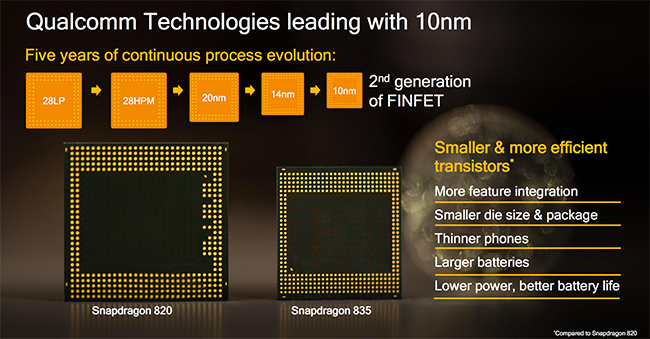
The Snapdragon 820 SoC was a significant milestone on Qualcomm’s roadmap. It was a solid improvement over the 808/810, delivering higher performance and efficiency, and became a commercial success, finding its way into the majority of flagship phones last year. More importantly, it heralded Qualcomm’s vision for mobile devices: heterogeneous computing. This meant new hardware—a much improved Hexagon 680 DSP that added single instruction, multiple data (SIMD) Hexagon Vector Extensions (HVX); Qualcomm’s first fully-custom 64-bit CPU core, Kryo, which focused on improving floating-point IPC; and an updated Adreno GPU with strong ALU performance—for enabling new software technologies and user experiences—artificial intelligence for smarter personal assistants, machine learning for object recognition, computational photography for better image and video quality, and new AR/VR experiences.
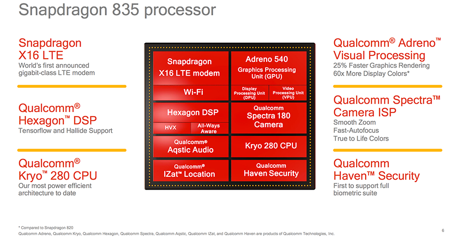
Snapdragon 835—now a part of Qualcomm’s Snapdragon Mobile Platform that includes all of the company’s mobile hardware and software—is an evolutionary product that builds on this vision. The greater than 3 billion transistor SoC is the first to use Samsung’s 10nm “10LPE” FinFET process, which reduces overall package size by 35% relative to Snapdragon 820. The new SoC’s CPU transplant and X16 LTE modem, which tops out at 1Gbps (Category 16) on the downlink, are the biggest changes, but most of the other blocks within the SoC have received at least minor updates too. For detailed information about all the changes and new features, you can read our Snapdragon 835 launch article.
| Qualcomm Snapdragon SoCs: Three Generations | |||
| SoC | Snapdragon 835 (MSM8998) |
Snapdragon 820 / 821 (MSM8996 / MSM8996 Pro) |
Snapdragon 810 (MSM8994) |
| CPU | 4x Kryo 280 Performance @ 2.45GHz 4x Kryo 280 Efficiency @ 1.90GHz |
2x Kryo @ 2.15GHz / 2.34GHz 2x Kryo @ 1.59GHz / 2.19GHz |
4x Cortex-A57 @ 2.00GHz 4x Cortex-A53 @ 1.50GHz |
| GPU | Adreno 540 @ 710MHz ? | Adreno 530 @ 624MHz / 653MHz | Adreno 430 @ 630MHz |
| Memory | 2x 32-bit @ 1866MHz LPDDR4x 29.9GB/s |
2x 32-bit @ 1866MHz LPDDR4 29.9GB/s |
2x 32-bit @ 1600MHz LPDDR4 25.6GB/s |
| ISP/Camera | Dual 14-bit Spectra 180 ISP 1x 32MP or 2x 16MP |
Dual 14-bit Spectra ISP 1x 25MP or 2x 13MP |
Dual 14-bit ISP 1x 21MP |
| Encode/Decode | 2160p30 (2160p60 decode), 1080p120 H.264 & H.265 |
2160p30 (2160p60 decode), 1080p120 H.264 & H.265 |
2160p30 (2160p60 decode), 1080p120 H.264 & H.265 |
| Integrated Modem | Snapdragon X16 LTE (Category 16/13) DL = 1000Mbps 3x20MHz CA, 256-QAM UL = 150Mbps 2x20MHz CA, 64-QAM |
Snapdragon X12 LTE (Category 12/13) DL = 600Mbps 3x20MHz CA, 256-QAM UL = 150Mbps 2x20MHz CA, 64-QAM |
Snapdragon X10 LTE (Category 9) DL = 450Mbps 3x20MHz CA, 64-QAM UL = 50Mbps 1x20MHz CA, 16-QAM |
| Mfc. Process | 10nm LPE | 14nm LPP | 20nm SoC |
In what has become an annual tradition going all the way back to Snapdragon 800, Qualcomm invited the media to its headquarters in San Diego for some feature demonstrations and limited testing using the company’s Mobile Development Platform (MDP) devices. These are fully functional tablets or smartphones in a slightly oversized, utilitarian chassis used for hardware testing and software development. The MDP for Snapdragon 810 took the form of a tablet, while Snapdragon 820 came inside a large smartphone with a 6.2-inch display. This downsizing trend continues for Snapdragon 835, whose MDP/S is a smartphone with 6GB of RAM, a 5.5-inch 2560×1440 display, and a small 2850 mAh battery. The use of a smaller chassis is encouraging, because it has less mass and surface area to absorb and dissipate heat. This suggests a lower TDP for the 835, but we’ll need to measure power consumption to be sure.
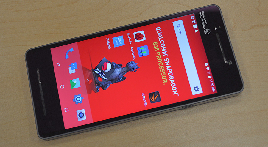
Because we only had a limited time for testing, we focused on running some basic CPU, GPU, and memory performance tests. Keep in mind that we were testing prototype hardware running pre-production software that resulted in a few hiccups. The condensed testing period also forced us to stray slightly from our usual testing methodology. Therefore, these numbers should be viewed as preliminary and could change by the time retail units begin shipping.
Snapdragon 820 included Qualcomm’s first fully-custom 64-bit CPU cores. The unique microarchitecture’s floating-point IPC was very good, but integer IPC was no better than ARM’s older A57 core. Its power efficiency was lower than competing cores as well. Instead of using a revised quad-core Kryo arrangement for Snapdragon 835, Qualcomm decided to go in a completely different direction.
The new Kryo 280, despite the similar name, shares no design DNA with the original Kryo. Its an octa-core, big.LITTLE configuration with four “performance” cores and four lower-power “efficiency” cores. What makes Kryo 280 unique, however, is that it’s the first design to use ARM’s new “Built on ARM Cortex Technology” (BoC) license, which allows vendors to customize ARM cores. This new semi-custom option gives vendors the ability to differentiate their products from those using ARM’s stock cores while avoiding the more costly route of creating a fully-custom design from scratch.
The BoC license allows the vendor to request certain modifications, particularly to the fetch block and issue queues, but certain parts of the microarchitecture are off limits, including the decoder and execution pipelines, because modifying these blocks requires too much effort. Qualcomm is not disclosing which ARM cores serve as the foundation for Kryo 280 or precisely which modifications it requested, but it did say that both CPU clusters use semi-custom cores. Qualcomm also confirmed that Snapdragon 835’s memory controllers are its own design.
| Geekbench 4 – Integer Performance Single Threaded |
|||
| Snapdragon 835 | Snapdragon 821 (% Advantage) |
Snapdragon 810 (% Advantage) |
|
| AES | 905.40 MB/s | 559.10 MB/s (61.9%) |
714.47 MB/s (26.7%) |
| LZMA | 3.13 MB/s | 2.20 MB/s (42.3%) |
1.92 MB/s (63.0%) |
| JPEG | 16.80 Mpixels/s | 21.60 Mpixels/s (-22.2%) |
12.27 Mpixels/s (36.9%) |
| Canny | 23.60 Mpixels/s | 30.27 Mpixels/s (-22.0%) |
23.63 Mpixels/s (-0.1%) |
| Lua | 1.84 MB/s | 1.47 MB/s (25.2%) |
1.20 MB/s (53.3%) |
| Dijkstra | 1.73 MTE/s | 1.39 MTE/s (24.5%) |
0.91 MTE/s (90.1%) |
| SQLite | 53.00 Krows/s | 36.67 Krows/s (44.5%) |
33.30 Krows/s (59.2%) |
| HTML5 Parse | 8.67 MB/s | 7.61 MB/s (13.9%) |
6.38 MB/s (35.9%) |
| HTML5 DOM | 2.26 Melems/s | 0.37 Melems/s (510.8%) |
1.26 Melems/s (79.4%) |
| Histogram Equalization | 52.90 Mpixels/s | 51.17 Mpixels/s (3.4%) |
53.60 Mpixels/s (-1.3%) |
| PDF Rendering | 50.90 Mpixels/s | 52.97 Mpixels/s (-3.9%) |
43.70 Mpixels/s (16.5%) |
| LLVM | 196.80 functions/s | 113.53 functions/s (73.3%) |
108.87 functions/s (80.8%) |
| Camera | 5.71 images/s | 7.19 images/s (-20.6%) |
4.69 images/s (21.7%) |
The Snapdragon 835’s Kryo 280 CPU shows a noticeable improvement in integer IPC relative to the 820/821’s Kryo core. This is not unexpected, however, considering integer performance was not one of Kryo’s strengths. While most workloads see large increases, there are a few regressions too, notably in JPEG, Canny, and Camera. We saw this same performance pattern from Kirin 960’s A73 CPU as well. These integer results, along with L1/L2 cache behavior, match the A73’s unique performance fingerprint, confirming that Kryo 280’s performance cores are based on ARM’s latest IP.
Quickly comparing Snapdragon 835 and Kirin 960 Geekbench 4 Integer results also shows performance variations that cannot be fully explained by differences in frequency or normal testing variance. The differences only occur in a few specific tests and range from 9% to -5%, which again is not completely unexpected given the limited number of modifications the BoC license allows for semi-custom designs.
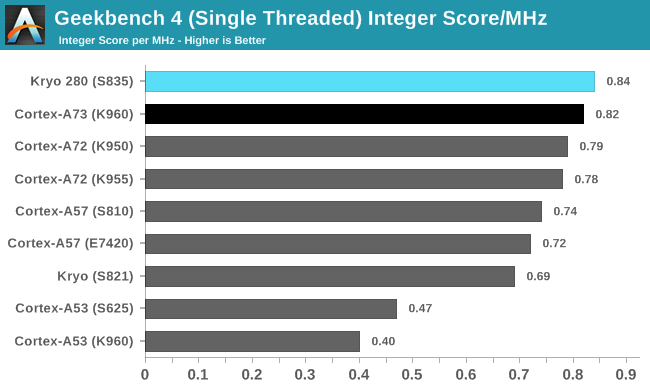
The chart above divides the overall integer score by CPU frequency, making it easier to directly compare IPC. Taken as a whole, the performance of Kryo 280’s semi-custom performance core is not much different than the Kirin 960’s A73 core in this group of workloads, with individual gains and losses nearly averaging out. Its overall IPC is also only about 6% higher than A72 and 14% higher than A57. Its advantage over Snapdragon 820/821 widens to 22%, partly because Kryo’s poor performance in the LLVM and HTML5 DOM workloads drags down its overall score.
While Snapdragon 835 leads other SoCs by a slim margin in this test, it’s not a sweeping victory. Just like we saw with Kirin 960’s A73 cores, performance improves in some workloads but regresses in others.
| Geekbench 4 – Floating Point Performance Single Threaded |
|||
| Snapdragon 835 | Snapdragon 821 (% Advantage) |
Snapdragon 810 (% Advantage) |
|
| SGEMM | 11.5 GFLOPS | 12.2 GFLOPS (-5.7%) |
11.0 GFLOPS (4.2%) |
| SFFT | 2.9 GFLOPS | 3.2 GFLOPS (-9.7%) |
2.3 GFLOPS (25.2%) |
| N-Body Physics | 879.6 Kpairs/s | 1156.7 Kpairs/s (-24.0%) |
580.2 Kpairs/s (51.6%) |
| Rigid Body Physics | 6181.7 FPS | 7171.3 FPS (-13.8%) |
4183.4 FPS (47.8%) |
| Ray Tracing | 232.6 Kpixels/s | 298.7 Kpixels/s (-22.0%) |
130.1 Kpixels/s (78.7%) |
| HDR | 7.8 Mpixels/s | 10.8 Mpixels/s (-27.6%) |
6.4 Mpixels/s (21.9%) |
| Gaussian Blur | 23.4 Mpixels/s | 48.5 Mpixels/s (-51.8%) |
21.9 Mpixels/s (6.7%) |
| Speech Recognition | 13.9 Words/s | 10.9 Words/s (27.5%) |
8.1 Words/s (71.4%) |
| Face Detection | 513.8 Ksubs/s | 685.0 Ksubs/s (-25.0%) |
404.4 Ksubs/s (27.0%) |
Snapdragon 835’s Kryo 280 takes two steps backwards when running Geekbench 4’s floating-point workloads, finishing well behind Snapdragon 820/821’s Kryo core and even a little behind SoCs using the A72 core. Its IPC is on par with the Kirin 960’s A73 core, with even less variation between individual scores than we saw when running the integer workloads.
The A73’s slight performance regression relative to the A72, which also applies to the semi-custom Kryo 280, is a bit surprising, because their NEON execution units are relatively unchanged from the A72’s design. If anything, the A73’s lower-latency front end and improvements to its fetch block and memory system should give it an advantage, but that’s not the case. The A73’s narrower decode stage could limit performance for some workloads but not all. Both the Kirin 960’s A73 and Snapdragon 835’s Kryo 280 show reduced L2 cache read/write bandwidth (and lower L1 write bandwidth) relative to A72, which could also negatively impact performance.
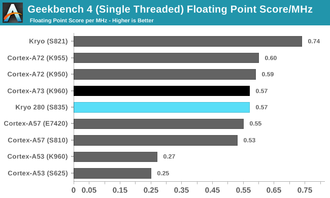
Snapdragon 835’s floating-point IPC is 23% lower than Snapdragon 820/821’s. One has to wonder if this is the result of a forced compromise or a willing change in design philosophy. When Qualcomm started work on Kryo more than 2 years ago, it may have envisioned new workloads that never materialized. Or it could be that with more compute workloads shifting to the GPU and DSP to improve efficiency, it was willing to sacrifice some floating-point performance to save area and power.
| Geekbench 4 – Memory Performance Single Threaded |
|||
| Snapdragon 835 | Snapdragon 821 (% Advantage) |
Snapdragon 810 (% Advantage) |
|
| Memory Copy | 4.70 GB/s | 7.82 GB/s (-39.9%) |
3.99 GB/s (17.8%) |
| Memory Latency | 13.95 Mops/s | 6.64 Mops/s (110.1%) |
4.29 Mops/s (225.2%) |
| Memory Bandwidth | 17.95 GB/s | 13.53 GB/s (32.7%) |
7.15 GB/s (151.0%) |
The Kryo 280, A73, A72, and A57 cores all have 2 address generation units (AGUs). Unlike the A72/A57, however, which use dedicated AGUs for load and store operations, each AGU in Kryo 280/A73 is capable of performing both operations. For Kirin 960, this change, among others, reduces memory latency and significantly improves bandwidth to main system memory relative to Kirin 950.
Snapdragon 835’s memory latency and bandwidth numbers are even better than Kirin 960’s—up to 11% after accounting for differences in CPU frequency. The 835 sees impressive gains over the 820/821 too. Switching to Kryo 280 does not provide the same bandwidth boost as the switch to A73 did for Kirin 960, however, because Kryo’s 2 AGUs were already capable of performing both load and store operations, albeit with a higher latency in some cases.
System Performance
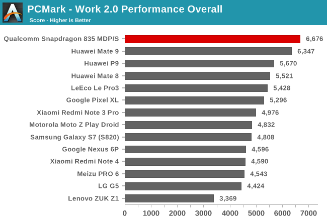
So far our initial results show Snapdragon 835’s Kryo 280 is a big.LITTLE combination of semi-custom A53 and A73 CPU cores, whose integer and floating-point IPC is similar to Kirin 960. System-level tests like PCMark, which includes several realistic workloads that stress the CPU, GPU, RAM, and NAND storage using standard Android API calls, are affected by more than just CPU IPC and memory latency, however. Device OEMs tune the software parameters that control the scheduler and DVFS systems to achieve the desired balance between performance and battery life, to meet quality of service goals, and to stay within a particular design’s thermal limits.
No doubt we’ll see performance vary among the upcoming Snapdragon 835 devices, just like we do with other SoCs, but for now we see Qualcomm’s 835 MDP/S with the top overall score in PCMark, just barely ahead of the Mate 9 and its Kirin 960 SoC. It’s also 23% faster overall than the top-performing Snapdragon 821 phone.
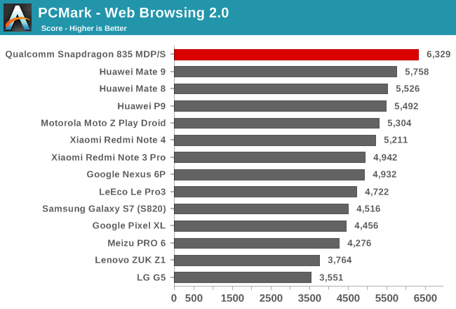
The Snapdragon 835 MDP/S performs well in the Web test, although its advantage over the Mate 9 is only 10%. Its performance lead over the Snapdragon 820/821 phones, which all fall behind SoCs using ARM’s A72 and A73 CPUs, grows to 34% in this integer-heavy test.
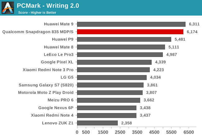
The PCMark Writing test generates frequent, short bursts of activity on the big CPU cores while performing a variety of operations, including PDF processing and file encryption (both integer workloads), memory operations, and even reading and writing some files to internal NAND. Because of this, it tends to produce the most varied results. Take the spread between the Snapdragon 820/821 phones, for example, where the LeEco Le Pro3 is 40% faster than the Galaxy S7 edge. The performance difference between the Snapdragon 835 MDP/S and Mate 9 is negligible, however. Comparing Snapdragon 835 to older members of the Snapdragon family reveals more significant differences; it’s 24% faster than the LeEco Le Pro3 (S821), 80% faster than the Nexus 6P (S810), and 162% faster than the Lenovo ZUK Z1 (S801AC).
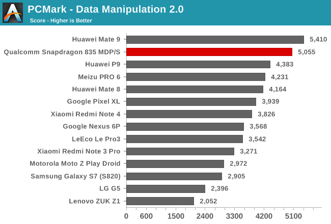
The PCMark Data Manipulation test is another primarily integer workload that measures how long it takes to parse chunks of data from several different file types and then records the frame rate while interacting with dynamic charts. Once again the Snapdragon 835 MDP/S and Mate 9 deliver similar performance, but they separate themselves a little further from the pack. Like we saw in the Writing test, the phones using Snapdragon 820 show significant performance variation, providing another example of how OEM tinkering impacts the user experience. The Snapdragon 835 MDP/S outperforms the Pixel XL by 28% and the LG G5 by 111%.
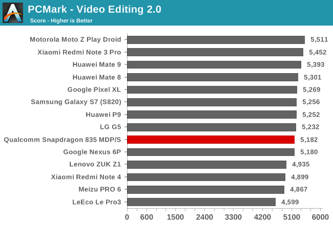
The Video Editing test, which uses OpenGL ES 2.0 fragment shaders for applying video effects, actually presents a very light load to the system. After monitoring the behavior of several phones while running this test, I’ve noticed that GPU frequency remains close to idle and most phones do not migrate threads to the big CPU cluster, using the little A53 cluster exclusively, which is why we see very little performance variation in this test.
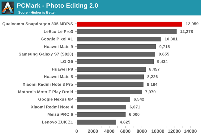
The Photo Editing test applies a number of different photo effects and filters with both the CPU and GPU. The Snapdragon 835 MDP/S and the phones using Snapdragon 820/821 rise to the top of the chart thanks to their Adreno GPU’s strong ALU performance. The 835’s Adreno 540 GPU helps it perform 33% better than the highest performing phone with an ARM GPU, the Mate 9 and its Mali-G71.
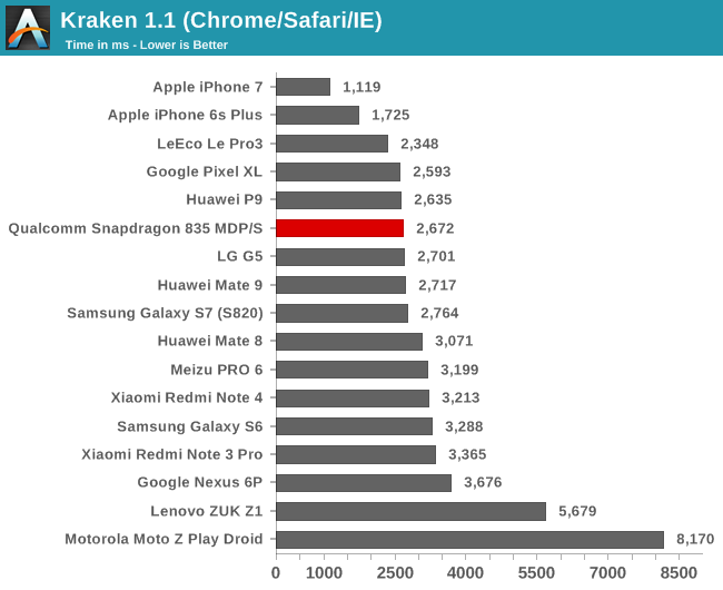
Yes, the iPhones perform well in these JavaScript tests. No, you cannot use these tests to compare IPC between Apple’s A-series SoCs and those found in Android phones, because they are running different browsers. A significant portion of the iPhones’ performance advantage actually comes from Safari’s JavaScript engine.
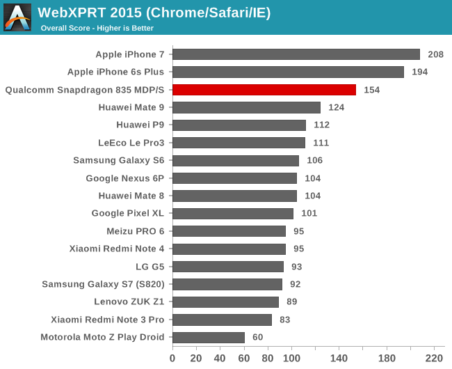
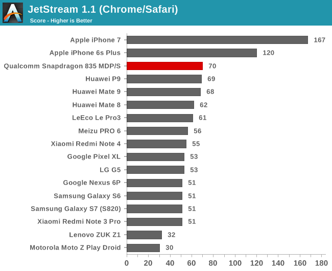
The Snapdragon 835 MDP/S compares favorably to other phones using the Chrome browser (all of the phones are using the latest version). It joins the Snapdragon 820/821 phones at the top of the chart in Kraken, although, its performance is no different. It essentially matches the Mate 9 in JetStream too, but pulls ahead of the Snapdragon 820/821 phones by 15% to 37%. Performance is unexpectedly good in WebXPRT 2015 where it pulls ahead of the Mate 9 by 24% and up to 67% over the Galaxy S7 (S820).
As an additional point of interest, and to further highlight the software layer’s effects, we also ran these tests using Qualcomm’s internally developed browser that’s optimized for Snapdragon SoCs. Kraken only sees a modest improvement to 2,305 ms, but JetStream improves by 24% to 87 and WebXPRT 2015 jumps to 280, an 82% improvement.
Snapdragon 835’s updated Adreno 540 GPU shares the same basic architecture as Snapdragon 820’s Adreno 530, but receives some optimizations to remove bottlenecks along with some tweaks to its ALUs and register file. The Adreno 540 also reduces the amount of work done per pixel by using improved depth rejection, which could further improve performance and reduce power consumption.
Qualcomm is claiming a general 25% increase in 3D rendering performance relative to the Adreno 530 in S820. While not officially confirmed, it appears that Qualcomm is using the move to 10nm to increase peak GPU frequency to 710MHz, a roughly 14% increase over S820’s peak operating point, which would account for a significant chunk of the claimed performance boost.
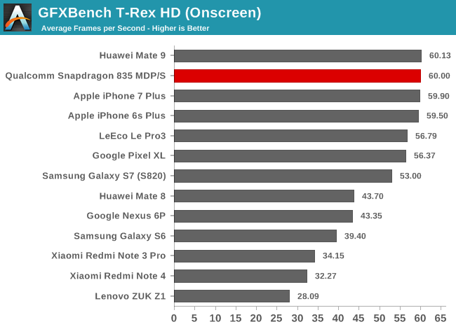
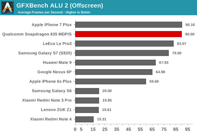
GFXBench T-Rex is an older OpenGL ES 2.0-based game simulation that’s not strictly limited by shader performance like the newer tests, which is one reason why flagship phones have been hitting the 60fps V-Sync limit for awhile now in the onscreen portion of the test. More recently, we’ve seen the iPhone 7 Plus and Mate 9, which both have 1080p displays, average 60fps over the duration of the test. Now the Snapdragon 835 MDP/S becomes the first 1440p device to reach this milestone.
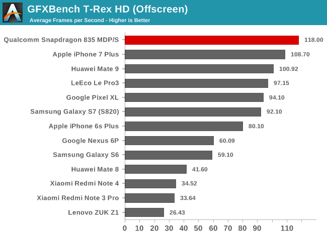
The Snapdragon 835 MDP/S outperforms the iPhone 7 Plus and Mate 9 when running offscreen at a fixed 1080p resolution. It’s also 25% faster than the Pixel XL, the highest performing Snapdragon 820 phone, exactly matching Qualcomm’s performance claim. Sliding a little further back along Adreno’s roadmap shows the Adreno 540 with almost a 2x advantage over the Nexus 6P’s Adreno 430 and a 4.5x advantage over the ZUK Z1’s Adreno 330.
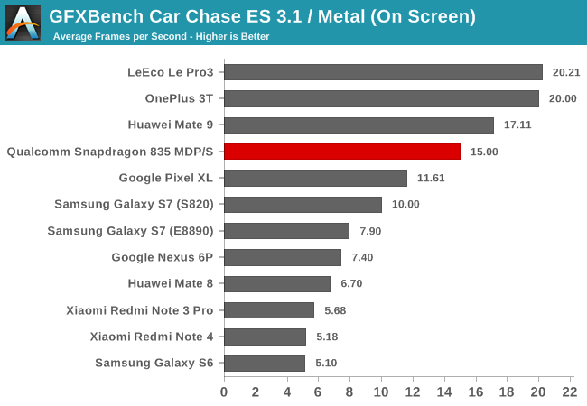
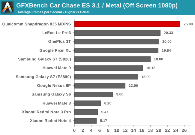
The GFXBench Car Chase game simulation uses a modern rendering pipeline with the latest features found in OpenGL ES 3.1 plus Android Extension Pack (AEP), including tessellation. Like many current games, it stresses ALU performance to deliver advanced effects.
Lower resolution 1080p displays paired with modern GPUs elevate the LeEco Le Pro3 (S821), OnePlus 3T (S820), and Huawei Mate 9 (Kirin 960) to the top of the chart in the onscreen portion of the test. The Snapdragon 835 MDP/S is the fastest 1440p device, besting the second-place Pixel XL by 29%.
Moving to the offscreen test shows the Adreno 540 GPU with a 25% lead over the Adreno 530 in S820. I do not usually put too much stock in performance claims on marketing slides, but so far Qualcomm’s claim is surprisingly accurate. Even more impressive is its 55% lead over the Mate 9’s Mali-G71MP8 GPU, which is based on ARM’s latest Bifrost microarchitecture and is running at 960MHz to 1037MHz during this test.
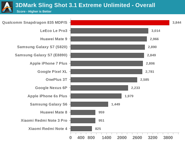
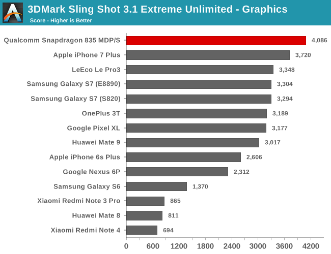
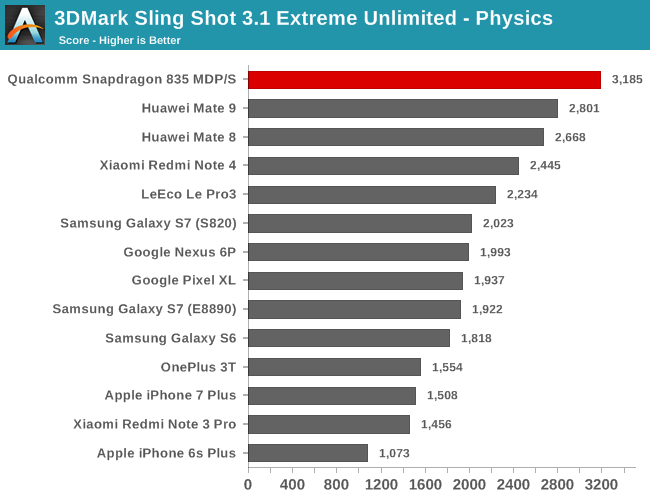
3DMark Sling Shot Extreme uses either OpenGL ES 3.1 on Android or Metal on iOS and stresses the GPU and memory system by rendering offscreen at 1440p (instead of 1080p like our other tests).
The Snapdragon 835’s 30% better overall score is pretty significant, considering that there’s only an 8% difference between all the phones using the Apple A10, Exynos 8890, Kirin 960, and S820/S821 SoCs. Diving into the graphics segment shows the Snapdragon 835 MDP/S outperforming the iPhone 7 Plus by 10% and both the S820 and Exynos 8890 versions of the Galaxy S7 by 24%.
Unlike the Adreno 530, which saw a significant uplift in geometry processing from changes to its microarchitecture, it does not appear that any additional changes were made to Adreno 540 based on its similar performance in 3DMark Sling Shot’s first graphics test. ARM’s Mali GPUs have done comparatively well in geometry processing tasks in the past, and in the first graphics test the Adreno 540 is only 11% faster than the Mate 9’s Mali-G71 GPU.
It’s in the second graphics test, which emphasizes shader performance, where we see the biggest gains from Adreno 540, with a 34% lead over the Galaxy S7’s Adreno 530 and a 50% lead over the Mate 9’s Mali-G71. Qualcomm’s changes to its ALUs and register file seem to pay dividends here.
The Physics test runs on the CPU and is heavily influenced by how well an SoC’s memory controllers handle random access patterns. The Snapdragon 835 MDP/S finishes ahead of the Mate 9 by 14% despite their similar CPU performance. The S835’s memory controllers deliver lower latency and higher bandwidth than Kirin 960’s, which could explain its better result in this test.
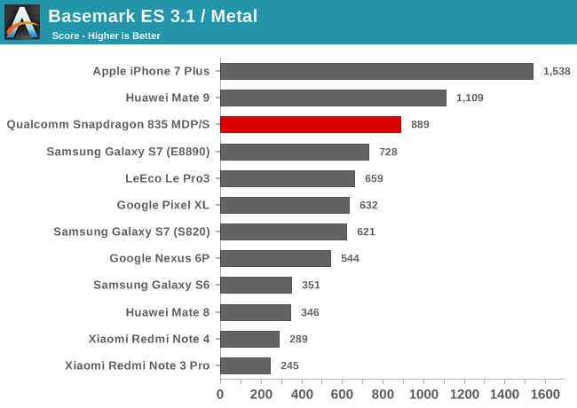
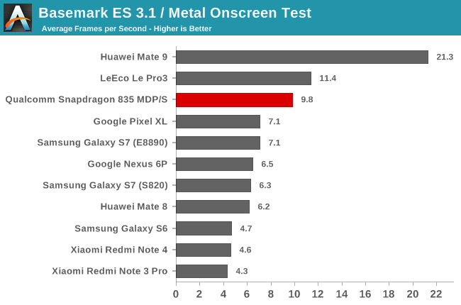
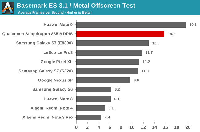
The Basemark ES 3.1 game simulation uses either OpenGL ES 3.1 on Android or Metal on iOS. It includes a number of post-processing, particle, and lighting effects, but does not include tessellation like GFXBench 4.0 Car Chase.
Until Vulkan support is added to benchmarks later this year, Android devices will continue to rely on OpenGL, putting them at a huge disadvantage to iPhones running Apple’s Metal graphics API, which dramatically reduces driver overhead when issuing draw calls. In this particular test, Metal helps push the iPhone 7 Plus in front of the Snapdragon 835 MDP/S by 73%.
ARM’s Mali GPUs perform better than their Adreno counterparts when running Basemark ES 3.1’s workloads; the Exynos 8890’s Mali-T880MP12 is 15% faster than S820’s Adreno 530 and Kirin 960’s Mali-G71MP8 is 25% faster than S835’s Adreno 540 in the offscreen test. The Snapdragon 835 MDP/S does perform 40% faster than the S820 in the Pixel XL, which is quite a bit more than the 25% gain it sees in our other tests.
The common theme in all of the game simulation tests is the Adreno 540’s better ALU performance, so I thought it would be interesting to see how well it performs in GFXBench’s synthetic ALU test. Surprisingly, its microarchitecture improvements are of no help here. The S835’s 14% advantage over the S820 and 8% advantage over the S821 exactly mirror their differences GPU frequency, assuming 710MHz for S835, suggesting this workload is bottlenecked elsewhere. It still manages to outperform the Mate 9’s Kirin 960 by 32%, however.
While the primary purpose of our visit out to Qualcomm’s offices was for benchmarking, for this year’s event Qualcomm went one step further and invited us to take a tour of some of their labs. The tour itself was plenty interesting (more on this in a bit), however arguably the more important aspect of the tour isn’t what we saw, but why Qualcomm is giving the press lab tours after so long. A tour may sound trite, but for Qualcomm it’s a sign of bigger things.
Perhaps the most important thing to understand about Qualcomm is that while the bulk of the company’s revenue comes from chips, the majority of their actual profits come from various technology and patent licensing programs. The actual breakdown between the two halves of Qualcomm gets a bit weird when trying to best account for which half foots the bill for R&D, but at the end of the day it’s Qualcomm’s licensing business that is making them the most money.
| Qualcomm Financials (FY’2016) | ||||
| Chip-Making | Licensing | |||
| Revenue | $ 15.4B | $ 7.6B | ||
| Profit (Pretax) | $ 1.8B | $ 6.5B | ||
As a result, if boardroom-level rumors are to be believed, the company is never quite sure how to balance the two businesses. Some groups want licensing and chip design separated, and others want them to stay combined. Qualcomm seems content to stick with the status quo and their $ 5.7B in profits for 2016, but as a consequence of this unusual split it means that the chip side of Qualcomm is always under a bit of pressure to prove itself.
The good news for the chip business is that it’s doing fairly well, especially in North America. Most high-end Android smartphones sold in the US are based on Qualcomm’s chips, Qualcomm’s modems are in some (but no longer all) of Apple’s iPhone SKUs, and even in the midrange market Qualcomm’s Snapdragon 600 series chips are in a number of popular phones. The flip side of this is that outside of the US and especially outside of the high-end, Qualcomm’s chip business is under constant pressure from both their partners and their competitors. Samsung is happy to stick with their own home-grown Exynos chips outside of North America, and other chip vendors like MediaTek nip at Qualcomm’s heels with competent midrange SoCs that are priced very aggressively. So while Qualcomm’s chip business is doing well right now, that could very well change in the future.
But what does this have to do with a press tour of their labs? One of the big initiatives for Qualcomm, as exemplified in last week’s Snapdragon branding tweak, is that the chip arm of the company wants to get away from being so frequently judged on the basis of their CPU and only their CPU. This is why Snapdragon is now a platform versus a processor, and similarly, it’s why we’re going to see Qualcomm increasingly talking up the other aspects of their SoCs in the future. Their SoCs and associated front-end hardware are more than just the Kryo CPU, and they want the world to know that.

For Qualcomm this move makes a lot of sense. CPU performance is still growing year-after-year, but as we’ve seen, those gains are plateauing some as a consequence of diminishing IPC gains and diminishing clockspeed gains. Meanwhile, although the Kryo is a customized CPU design, as we’ve seen in our benchmark data it doesn’t behave radically different from ARM’s Cortex-A72 and Cortex-A73 designs that other vendors can license. Short of a “Cyclone” moment for Qualcomm, their CPU performance is close enough to the rest of the Android pack that they can’t clearly stand out from other vendors in the way Apple can. And that means they need to promote and sell their SoCs as the sum of their parts, and not just a CPU with a bunch of extra stuff bolted on.

This also means that even though Qualcomm is one of the first vendors to ship a 10nm high-end SoC – and enjoying the performance benefits thereof – we’re also going to see the company downplay benchmarks a bit for not capturing the complete “end-user experience.”

And to the company’s credit, they aren’t wrong. CPU, GPU, and memory performance are all easy enough to test, vary a great deal among SoC designs, and are similarly easy to communicate. DSPs, ISPs, and other aspects are not nearly as easy to test, never mind communicating those advantages to a wider audience.
Still, once we get outside of CPU/GPU/memory and into other functional blocks of a SoC, things get murkier for everyone. A video decode block may as well be a static piece of hardware – as long as it does its job well, no one will notice – and a great Wi-Fi radio can be kneecapped by a bad device design. So as much as Qualcomm wants to push the broader end-user experience, they will never completely escape the fact that the core features of their SoCs will be the first to be put to the test, and that wider testing is going to be less meaningful to customers, or more practically speaking outside the budgets of technology journalists.
In any case, let’s talk about the tour itself. A first for Qualcomm, the company has given us a bit of access to show off some of the aspects of their SoCs we can’t easily measure ourselves, or to show off other parts of the Snapdragon platform (such as the software stack) that can’t be empirically measured. Given that Qualcomm has historically kept to themselves and been hesitant to engage with tech journalists, even a limited tour is a notable shift for the company. Not to mention a promising sign that, if nothing else, they better understand that the work their engineers and other staff put into products like the Snapdragon 835 deserves to be in the spotlight as well. The idea that engineering is cool isn’t just a STEM educational platform, but something we at AnandTech experience week in and week out.

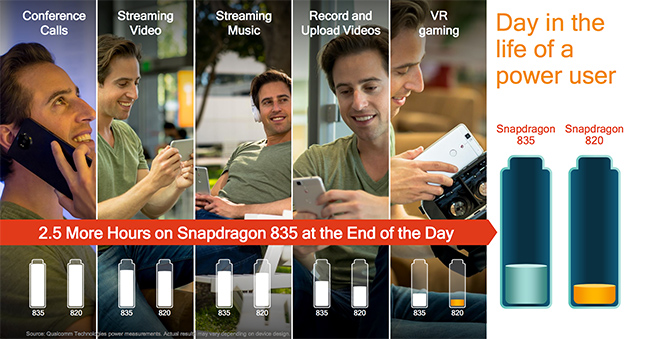
Power Lab
Given that Qualcomm’s meeting room for press testing was only setup to test performance and not power consumption, it was only fitting that the company’s tour started at their power lab. Here, director of product management Johnny John had setup a demo comparing the power consumption of Snapdragon 820 versus 835. While the usual caveats apply – mainly, that this was a prearranged demo that we didn’t control – it none the less suitably highlights both the power consumption improvements of 835, and Qualcomm’s direction with balancing power consumption with performance for the new SoC.
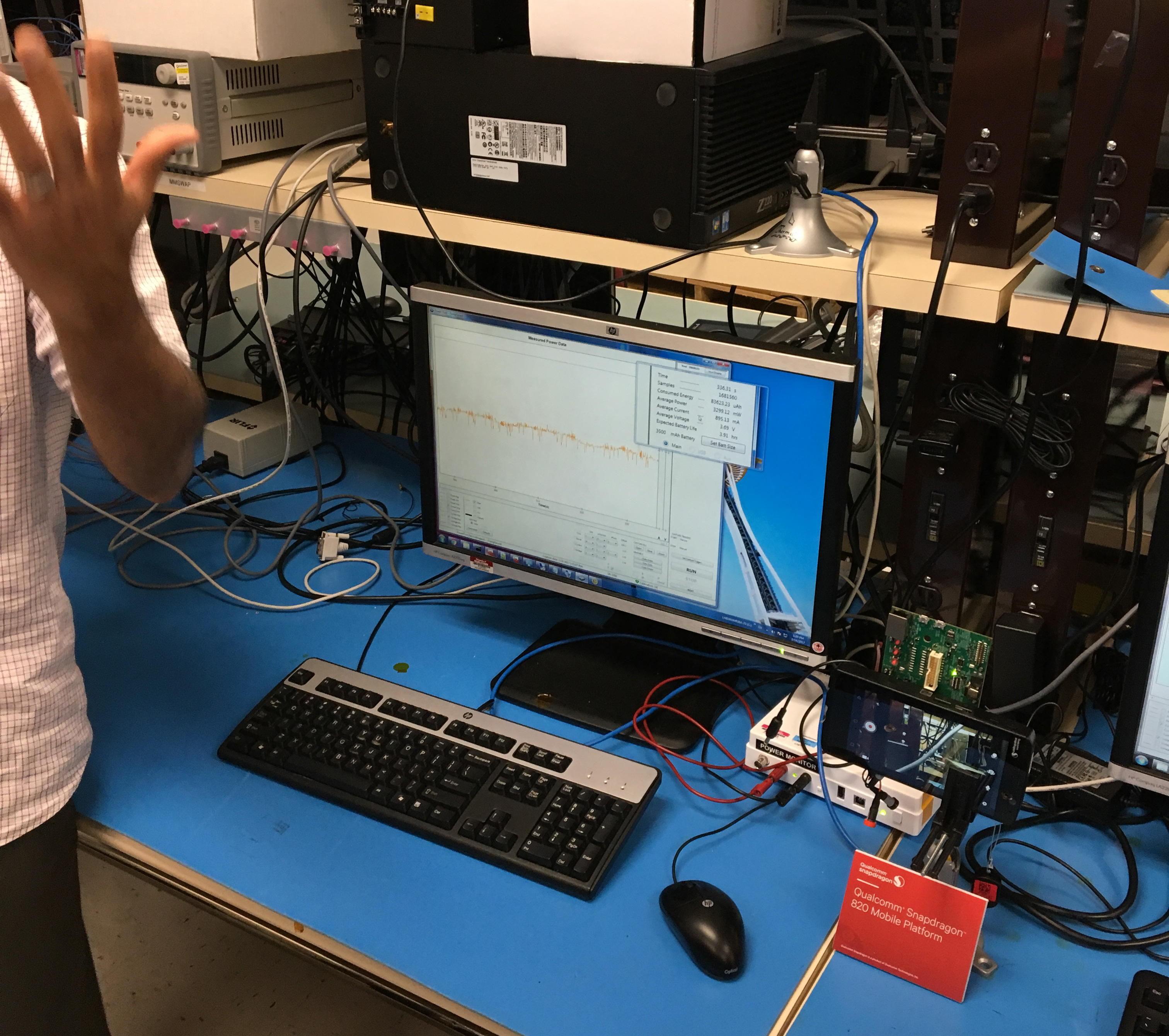
For this demo, Qualcomm set up otherwise identical development phones running the SD820 and SD835 respectively. Both were running the same fixed VR workload as an example of a high power consumption task. Since this was a fixed workload, the faster SD835 phone in turn gets to bank the entirety of its advantage in power savings. Meanwhile to measure power consumption, Qualcomm’s power measurement gear tapped into the phones at the battery level, so these are phone-level measurements.

| Qualcomm Power Testing – Device Level w/Fixed Workload | |||
| Power Consumption | |||
| SD820 Reference Phone | 4.60W | ||
| SD835 Reference Phone | 3.56W | ||
The end result had the SD820 phone drawing an average of 4.6W, while the SD835 phone was drawing 3.56W, a power reduction of 23%. Real world use cases won’t be fixed workloads, so the power gains won’t be quite as great, but it shows where Qualcomm’s customers can go in configuring their devices. And indeed, Qualcomm’s own reference devices seem to be tuned a bit more towards power savings than performance, going hand-in-hand with the SoC size reduction that Qualcomm has also gone for with their new SoC. Customers make the final call, but Qualcomm seems to be nudging customers towards using their 10nm gains to curb power consumption more than improve performance.
Graphics & VR
The second stop on Qualcomm’s tour was what they call their Snapdragon Advanced Content Lab. This lab’s focus was on graphics and AR/VR development, though as the polar opposite of a Spartan lab or meeting room, “den of geeks” may be the better description.
![]()
To be honest, coming off of CES and GDC, Qualcomm’s advanced content group didn’t have much new to show off. The company is continuing to focus on getting Snapdragon SoCs into VR/AR headsets, and has been producing demos, hardware prototypes, and software toolsets to that end, all of which they have been showing off at the aforementioned trade shows. This is essentially the backend heavy-lifting that Qualcomm is doing to enable devices like the Pico Neo CV that we saw at GDC this year.

Along those lines, the company is also keen on showing off the software side of the equation with their performance profiling tools. The nuances are admittedly more something a developer is going to appreciate than an end-user, but it is a prime example of why the company is eager to brand Snapdragon as a platform as opposed to a processor. In the long run, they expect that software will become a much greater part in defining the overall platform.

Camera Lab
Our third stop was the company’s camera testing lab, which although was primarily demonstrating well-known methods for camera testing, was impressive in scope and price tag (ed: especially to tech journalists who would kill for similar equipment for phone reviews). The takeaway, at a high level, is that Qualcomm wants to show off the rigors of their testing methodology, and that every decision they make with their ISPs and associated software are based on significant empirical testing.

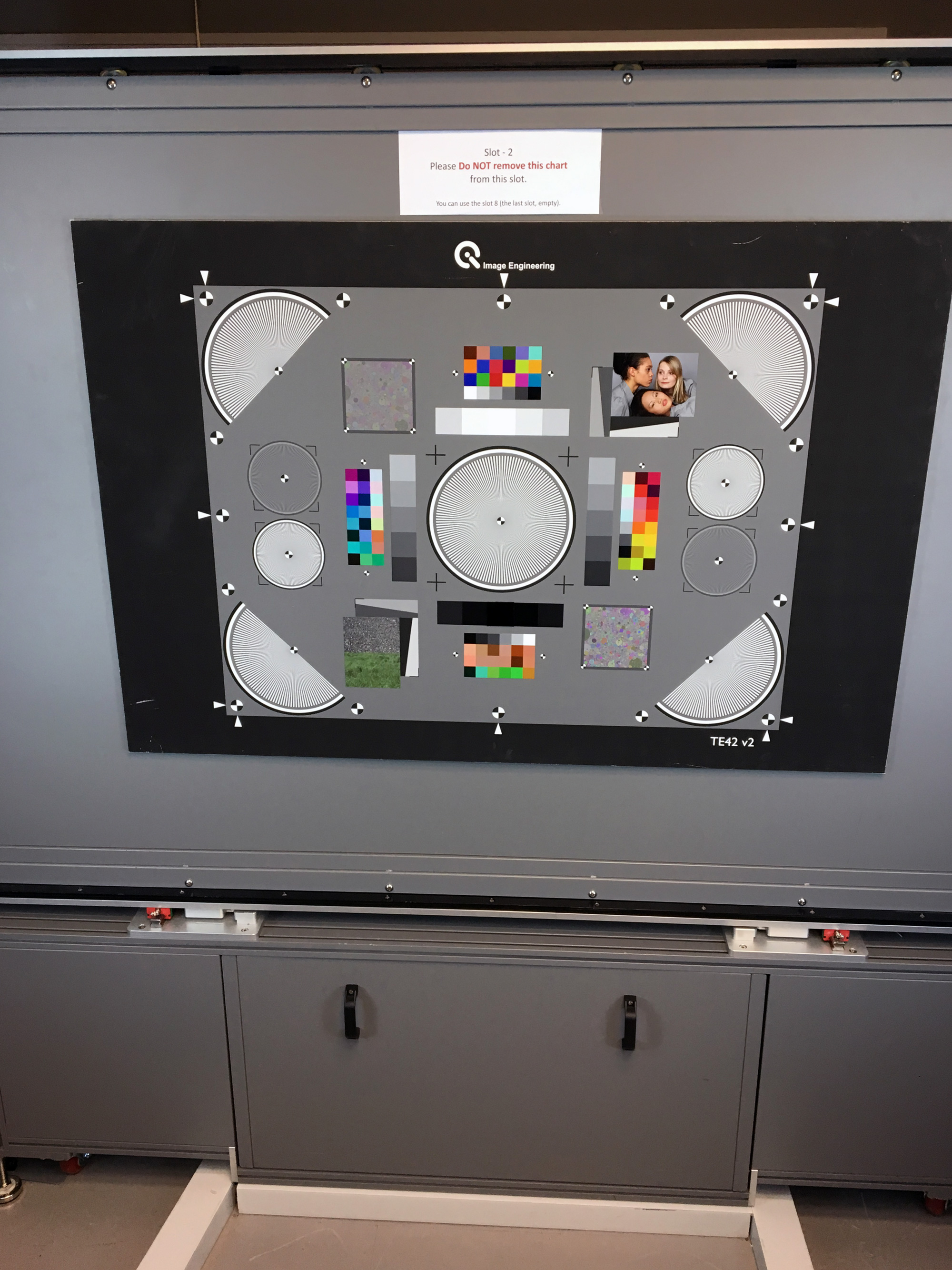
On the photo side of matters, the company has a few interesting tools at their disposal, the most useful likely being their variable lighting system, a pair of massive light cabinets that can generate light at a range of intensities and color temperatures. And though it may sound trivial, as our own Joshua Ho can attest to first-hand, this kind of consistent, systematic testing is not easy to do.

Meanwhile for testing the EIS capabilities of their ISP, Qualcomm has a specialized rig just for shaking phones. The particular ability that makes this rig noteworthy is that it can shake a phone using a pre-determined, tightly timed sequence, so that engineers can go back and see how well their EIS system handled specific motions. The ultimate goal here is to tweak their algorithms to produce good EIS results across a variety of scenarios, so that in average use cases the phone isn’t struggling to stabilize video.
Snapdragon Demo Room
The final stop on Qualcomm’s lab tour was what the company refers to as the Snapdragon Demo Room – which is to say that the company had rolled out a number of experience-based demos to show off various non-benchmark related aspects of their SoCs. This included audio, computer vision, and of course, LTE.

In recent months Qualcomm has been pushing the advantages of higher performance LTE modes, which in turn are the basis of what Qualcomm is branding as Gigabit LTE. The most recent LTE categories are leveraging both carrier aggregation and higher-order QAM modes, namely, 256-QAM. These higher-order modes require greater signal-to-noise ratios to be properly received, but in return allow a signal to carry more data, improving the total throughput of the network. The key point of Qualcomm’s simulations being that even with the tighter requirements of Category 16, it’s useful enough of the time to have a meaningful impact on improving spectral efficiency/reducing network (airtime) loads. Though, as I’m sure Qualcomm is painfully aware, putting theory into practice means getting carriers to upgrade their networks to support higher LTE categories.

One particularly interesting demo, even if things didn’t actually go quite according to plan, was iris scanning/recognition on a SD835 reference phone. Manufacturers have been toying with iris scanning as an alternative for fingerprint unlocking for a bit now, both as a means to remove the relatively large fingerprint sensor from their bezels and to offer a means for unlocking a phone that doesn’t require one’s hands. With the latest rendition of the technology, Qualcomm was eager to show off the improvements in the technology, as well as reiterate its security. The result was something of a wash; the demo worked very well with the product manager, but the phone couldn’t see/recognize my irises consistently enough to unlock the phone (ed: or perhaps Ryan is just soulless). Which this being a prototype, problems are not unexpected, but it’s a reminder that the tech hasn’t had the same number of development cycles as more proven fingerprint scanning technology.

On the flip side of the coin, how well the phone can see the rest of the world is also a subject of interest to Qualcomm. Computer vision/object detection demos aren’t new, but like other players in the industry, Qualcomm is lining up behind the recent advances in machine learning. By being able to efficiently executer (infer) highly trained neural networks, they hope to be able to do things faster and other new things entirely than what traditional computer vision has been capable of doing.

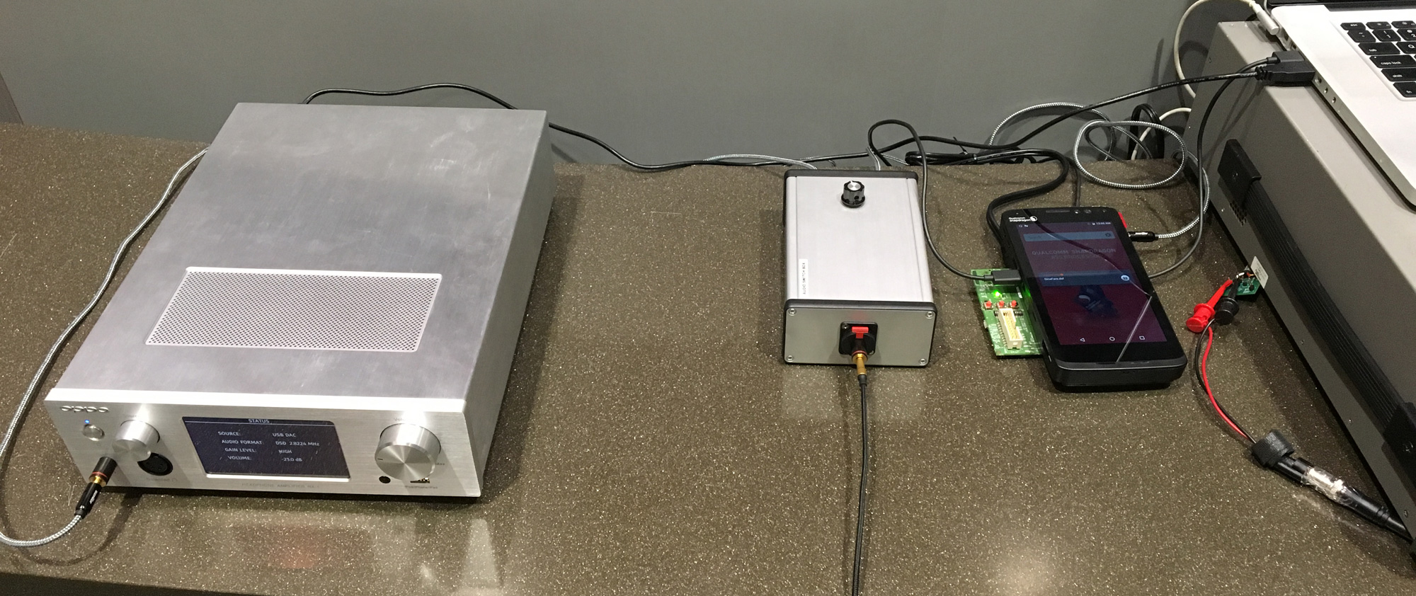
Finally, the company was also showing off their audio efforts, both on the playback and recording sides. On the former, they had an A/B setup between a phone and a dedicated receiver to show off the audio quality of the Snapdragon’s audio codecs and DAC, reiterating that at this point a properly designed phone should be able to keep up with dedicated audio gear for non-audiophiles, even with CD (or better) audio quality. Meanwhile on the audio input side, the company was showing off their improved voice activation capabilities for Snapdragon 835. While speed was hit & miss – both the SD835 and SD820 phones often responded in around the same time – over the day the company had recorded the newer phone as more frequently recognizing the activation phrase than the older phone.
Overall, while Qualcomm can’t easily quantify most of these experiences, it’s exactly these kinds of experiences that the company is wanting to bring to the forefront of the public’s mind, in order to show how Snapdragon is a platform, and to differentiate it from other SoCs. Just how much success they will have at this remains to be seen, but in the long run how successful they are here stands to have a significant impact in how the company’s chip-design arm presents itself to the world at large, and how it advertises its wares.
Mobile SoCs are packed with specialized processors: CPU, GPU, high-performance DSP (compute), low-power DSP (sensor hub), modem DSP (signal processing), ISP (image processing), fixed-function blocks (video, audio), etc. And while all of these pieces contribute to the overall user experience, some of them are difficult to quantify. The CPU and GPU remain vital to device performance and battery life, so it’s still important to probe their capabilities.
Chip Sizes Accurate to Scale
Our initial testing shows that Snapdragon 835’s Kryo 280 CPU is an octa-core, big.LITTLE configuration with four semi-custom A73 “performance” cores and four semi-custom A53 “efficiency” cores. Kryo 280’s performance cores are pretty much equivalent to Kirin 960’s A73 cores in both integer and floating-point IPC, but comparing them to Snapdragon 820’s Kryo CPU shows mixed results: integer IPC improves but floating-point regresses.
In our limited system testing, the Snapdragon 835’s IPC gains outweigh its losses, providing better overall performance than the Snapdragon 820/821 phones. Unsurprisingly, the Snapdragon 835 MDP/S matched the performance of the Mate 9’s Kirin 960, which may not sound all that exciting, but considering our positive experience with the Mate 9, it’s certainly not bad either.

Qualcomm continues to push hard into VR/AR, not just with smartphones but stand-alone HMDs too. The high resolution and low latency requirements for these experiences suddenly make the GPU a bottleneck once again. The Snapdragon 835’s updated Adreno 540 GPU, through a combination of microarchitecture tweaks and a higher peak operating frequency, is another evolutionary step along the VR path, delivering a 25% peak performance boost over Snapdragon 820’s Adreno 530.
As noted earlier, all of these results came from pre-production hardware and software that’s under Qualcomm’s control, so performance could still go up or down once retail units begin shipping; however, based on these preliminary numbers and feature additions, the Snapdragon 835 looks like a solid evolutionary upgrade over the S820. The one glaring omission in this initial assessment, though, is power efficiency, which is critical to both battery life and sustained performance. The potential power savings from the move to 10nm and the CPU swap could have a larger impact on user experience than the small performance gains and new features.
Autore: AnandTech