
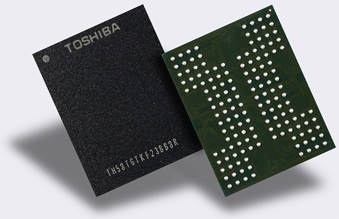
Toshiba last week announced its first 3D NAND flash memory chips featuring QLC (quadruple level cell) BiCS architecture. The new components feature 64 layers and developers of SSDs and SSD controller have already received samples of the devices, which Toshiba plans to use for various types of storage solutions.
Toshiba’s first 3D QLC NAND chips feature 768 Gb (96 GB) capacity and uses 64 layers, just like the company’s BICS3 chips with 256 Gb and 512 Gb capacities launched in 2016 and 2017. Toshiba does not share further details about its 3D QLC NAND IC (integrated circuit), such as page size, the number of planes as well as interface data transfer rate, but expect the latter to be high enough to build competitive SSDs in late 2018 to early 2019 (that’s our assumption). Speaking of applications that Toshiba expects to use its 3D QLC NAND ICs, the maker of flash memory mentions enterprise and consumer SSDs, tablets and memory cards.
Endurance++
Besides intention to produce 768 Gb 3D QLC NAND flash for the aforementioned devices, the most interesting part of Toshiba’s announcement is endurance specification for the upcoming components. According to the company, its 3D QLC NAND is targeted for ~1000 program/erase cycles, which is close to TLC NAND flash. This is considerably higher than the amount of P/E cycles (100 – 150) expected for QLC by the industry over the years. At first thought, it comes across a typo – didn’t they mean 100?. But the email we received was quite clear:
– What’s the number of P/E cycles supported by Toshiba’s QLC NAND?
– QLC P/E is targeted for 1K cycles.
It is unclear how Toshiba managed to increase the endurance of its 3D QLC NAND by an order of magnitude versus initially predicted. What we do know is that signal processing is more challenging with QLC than it is with TLC, as each cell needs to accurately determine sixteen different voltage profiles (up from 2 in SLC, 4 in MLC, and 8 in TLC).

The easiest way to handle this would be to increase the cell size: by having more electrons per logic level, it is easier to maintain the data and also read from it / write to it. However, the industry is also in a density race, where bits ber mm^2 is an issue. Also, to deal with read errors from QLC memory, controllers with very advanced ECC capabilities have to be used for QLC-based SSDs. Toshiba has its own QSBC (Quadruple Swing-By Codes) error correction technique, which it claims to be superior to LDPC (low-density parity-check) that is widely used today for TLC-powered drives. However, there are many LDPC implementations and it is unknown which of them Toshiba used for comparison against its QSBC. Moreover, there are more ECC methods that are often discussed at various industrial events (such as FMS), so Toshiba could be using any or none of them. The only thing that the company tells about its ECC now is that it is stronger than 120 bits/1 KB used today for TLC. In any case, if Toshiba’s statement about 1000 P/E cycles for QLC is correct, it means that that the company knows how to solve both endurance and signal processing challenges.
The main advantage of QLC NAND is increased storage density when compared to TLC and MLC, assuming the same die size. As was perhaps expected, die size numbers were not provided. However, last year Toshiba and Facebook talked about a case study QLC-powered SSD with 100 TB of capacity for WORM (write once read many) applications and it looks like large-capacity custom drives and memory cards will be the first to use QLC for cold storage. P/E cycles and re-write endurance isn’t a concern for WORM at this stage.
Toshiba has begun to sample its 3D QLC NAND memory devices earlier this month to various parties to enable development of SSDs and SSD controllers. Taking into account development and qualification time, Toshiba plans to mass produce its BiCS3 768 Gb 3D QLC NAND chips around the same time it starts to make its the next generation BiCS4 ICs. The latter is set to hit mass production in 2018, but the exact timeframe is yet to be determined.
Related Reading:
- Western Digital Announce BiCS4 3D NAND: 96 Layers, TLC & QLC, Up to 1 Tb per Chip
- Toshiba Selects Japan-U.S. Consortium As Preferred Buyer For Memory Business
- Toshiba Introduces XG5 Client NVMe SSD
- Western Digital Ships Client SSDs Based on 512 Gb 3D TLC NAND Chips
- Toshiba Samples 64-Layer 512 Gb BiCS 3D NAND, Announces 1 TB BGA SSD
- Toshiba Finalizes Plans for New 3D NAND Fab: Coming Online in 2019
Autore: Anton Shilov AnandTech
